


 It’s Only Common Sense: OCCAM—the Time Is Now
 Marcy's Musings: The Growing Industry
 Dan’s Biz Bookshelf: Seeing the How
Measuring the Temperature of Two-Dimensional Materials at the Atomic Level
February 5, 2018 | University of Illinois at ChicagoEstimated reading time: 3 minutes
Researchers at the University of Illinois at Chicago describe a new technique for precisely measuring the temperature and behavior of new two-dimensional materials that will allow engineers to design smaller and faster microprocessors.
Newly developed two-dimensional materials, such as graphene — which consists of a single layer of carbon atoms — have the potential to replace traditional microprocessing chips based on silicon, which have reached the limit of how small they can get. But engineers have been stymied by the inability to measure how temperature will affect these new materials, collectively known as transition metal dichalcogenides, or TMDs.
Using scanning transmission electron microscopy combined with spectroscopy, researchers at UIC were able to measure the temperature of several two-dimensional materials at the atomic level, paving the way for much smaller and faster microprocessors. They were also able to use their technique to measure how the two-dimensional materials would expand when heated.
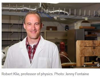
“Microprocessing chips in computers and other electronics get very hot, and we need to be able to measure not only how hot they can get, but how much the material will expand when heated,” said Robert Klie, professor of physics at UIC and corresponding author of the paper. “Knowing how a material will expand is important because if a material expands too much, connections with other materials, such as metal wires, can break and the chip is useless.”
Traditional ways to measure temperature don’t work on tiny flakes of two-dimensional materials that would be used in microprocessors because they are just too small. Optical temperature measurements, which use a reflected laser light to measure temperature, can’t be used on TMD chips because they don’t have enough surface area to accommodate the laser beam.
“We need to understand how heat builds up and how it is transmitted at the interface between two materials in order to build efficient microprocessors that work,” said Klie.
Klie and his colleagues devised a way to take temperature measurements of TMDs at the atomic level using scanning transition electron microscopy, which uses a beam of electrons transmitted through a specimen to form an image.
“Using this technique, we can zero in on and measure the vibration of atoms and electrons, which is essentially the temperature of a single atom in a two-dimensional material,” said Klie. Temperature is a measure of the average kinetic energy of the random motions of the particles, or atoms that make up a material. As a material gets hotter, the frequency of the atomic vibration gets higher. At absolute zero, the lowest theoretical temperature, all atomic motion stops.
Klie and his colleagues heated microscopic “flakes” of various TMDs inside the chamber of a scanning transmission electron microscope to different temperatures and then aimed the microscope’s electron beam at the material. Using a technique called electron energy-loss spectroscopy, they were able to measure the scattering of electrons off the two-dimensional materials caused by the electron beam. The scattering patterns were entered into a computer model that translated them into measurements of the vibrations of the atoms in the material – in other words, the temperature of the material at the atomic level.
“With this new technique, we can measure the temperature of a material with a resolution that is nearly 10 times better than conventional methods,” said Klie. “With this new approach, we can design better electronic devices that will be less prone to overheating and consume less power.”
The technique can also be used to predict how much materials will expand when heated and contract when cooled, which will help engineers build chips that are less prone to breaking at points where one material touches another, such as when a two-dimensional material chip makes contact with a wire.
“No other method can measure this effect at the spatial resolution we report,” said Klie. “This will allow engineers to design devices that can manage temperature changes between two different materials at the nano-scale level.”
Xuan Hu, Poya Yasaei, Jacob Jokisaari, Serdar Ogut and Amin Salehi-Khojin of the University of Illinois at Chicago, are co-authors of the paper.
This research was supported by EFRI 2-DARE grant 1542864 from the National Science Foundation.
Share on:


Suggested Items
Groundbreaking Ceremony Marks the Beginning of a New Era for Newccess Industrial; The Construction of the MINGXIN Building
04/12/2024 | Newccess IndustrialOn a clear and sunny day in March, the groundbreaking ceremony for the MINGXIN Building took place in Shenzhen, China. This moment marked the official commencement of construction for a project that will reshape the semiconductor materials industry.
The Need for a Holistic Global Sustainability Standard
04/10/2024 | Michael Ford, Aegis SoftwareNo one can deny that the resources of our fragile planet are finite. The environment seems like a third party, subject to constant degradation. We’re acutely aware of the effects of pollution on our climate, and despite our “throw-away” culture, recycling and recovery of materials has remained relatively expensive, even as we use more energy just to survive.
iNEMI Publishes Four Roadmap Topics
04/04/2024 | iNEMIThe International Electronics Manufacturing Initiative (iNEMI) announces the availability of the first roadmap topics in the new iNEMI Roadmap format. Printed circuit boards, sustainable electronics, smart manufacturing, and mmWave materials and test are now available online.
Insulectro’s 'Storekeepers' Extend Their Welcome to Technology Village at IPC APEX EXPO
04/03/2024 | InsulectroInsulectro, the largest distributor of materials for use in the manufacture of PCBs and printed electronics, welcomes attendees to its TECHNOLOGY VILLAGE during this year’s IPC APEX EXPO at the Anaheim Convention Center, April 9-11, 2024.
Checking In With ICAPE Group
04/03/2024 | Nolan Johnson, I-Connect007ICAPE Group’s field application engineer Erik Pederson drills down on sustainability, supply chain resiliency, and what value engineering really looks like in this exclusive interview. Founded in 1999, European-based ICAPE Group provides 21 million printed circuit boards and over six million technical parts to manufacturers every month. With 30 PCB manufacturing partners globally and 50 partners providing a wide array of technical parts, ICAPE Group has operations in China, Taiwan, Thailand, South Korea, Vietnam, South Africa, Europe, Mexico, and the United States. The company also focuses on the value proposition for its customers.