


 It’s Only Common Sense: OCCAM—the Time Is Now
 Marcy's Musings: The Growing Industry
 Dan’s Biz Bookshelf: Seeing the How
Building Miniature Optical Antennas Using DNA as a Guide
February 5, 2018 | University of JyväskyläEstimated reading time: 2 minutes
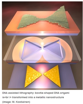
A new fabrication technique combines programmable DNA origami shapes and conventional lithography methods to create metallic nanoantennas and chiral shapes for diverse applications.
Research groups from University of Jyväskylä and Aalto University (Finland) together with researchers from California Institute of Technology (Caltech, USA) and Aarhus University (iNANO Center, Denmark) have reported a new highly parallel technique to fabricate precise metallic nanostructures with designed plasmonic properties by means of different self-assembled DNA origami shapes. The so-called DALI (DNA-assisted lithography) method has been published in the latest issue of Science Advances.
“We can build virtually any nanoscale shape using a DNA origami technique, and now we have shown how to use these accurate shapes as “stencils” to create millions of fully metallic nanostructures with 10 nm feature sizes in one go”, explains Adjunct Professor Veikko Linko from Aalto University. The trick in the DALI method is that when the DNA structures are deposited on a chip coated with silicon, silicon oxide can be selectively grown only on the bare areas of the substrate. “By controlling this process, we can create origami-shaped openings on the grown silicon oxide layer, and this layer can be used as a mask for the following lithography steps. Finally, we evaporate metal through these openings and create metallic structures having the same shape and size as the original DNA origami on a transparent substrate, such as sapphire”, Boxuan Shen from the Nanoscience Center of University of Jyväskylä describes the method.
The tiny metallic features cover the whole transparent substrate, and therefore these surfaces have intriguing optical properties. The small dimensions of the structures – in the range of ten nanometers – allow further tuning of these properties at the visible wavelength range. “Actually, we have demonstrated here a structure that we believe is the world’s smallest entirely metallic bowtie-shaped antenna. This extremely small size extends the operating range of optical features from infrared to visible”, states Adjunct Professor Jussi Toppari from Molecular Electronics and Plasmonics group at University of Jyväskylä. These antennas can find use in dozens of optical and plasmonic applications, such as surface enhanced Raman spectroscopy, biosensing or fluorescence enhancement. Moreover, the researchers demonstrated that the surfaces can be used as polarizers by fabricating chiral structures using DALI.
“The DALI method is highly parallel, and it could further enable cheap wafer-scale production of surfaces as it does not rely on costly patterning methods. It is also equipped for the future studies to provide bioinspired surfaces and metamaterials if the customized origami structures can be arranged on the substrate before metallization”, envisions Professor Mauri Kostiainen from the Biohybrid Materials Group at Aalto University.
Share on:


Suggested Items
Real Time with... IPC APEX EXPO 2024: all4-PCB, A Premier Solution Provider for the PCB Industry
04/22/2024 | Real Time with...IPC APEX EXPOIn the PCB industry, all4-PCB, is a top-tier equipment supplier and process solution provider. Ralph Jacobo highlights the active market and the demand for high-quality equipment, discusses their existing customers, investment in advanced substrates, and smaller board shops.
PCB007 Magazine April 2024 — The Growing Industry Issue
04/15/2024 | I-Connect007 Editorial TeamAfter more than two decades of steady decline in the U.S., the PCB industry is finally growing in the West thanks to the CHIPS and Science Act, DoD funding, and hopefully, the passing of HR 3249, the Printed Circuit Board and Substrates Act. The U.S. is now in a race to regain what was lost and then some. But what does “growing” look like for the organizations that have received DoD funding, and for the rest of us? How can we sustain this growth?
Paul Cooke of Ventec Talks About Glassless Revolution, High Reliability
04/09/2024 | Marcy LaRont, PCB007 MagazineMarcy LaRont from I-Connect007 caught up with Paul Cooke from Ventec at the SMTA UHDI Symposium on March 26 in Arizona. Paul discusses the challenges in developing future product lines for extremely high density, high reliability manufacturing, and focuses on the transition from glass to glassless substrate technology. He explains the advantages of using pure resin systems, enabling fabricators to create thinner materials for micro vias.
SCHMID Group Presents Breakthrough Solutions for Substrate Production at ISES USA
04/09/2024 | SCHMID GroupThe SCHMID Group, a global leader in providing solutions to the high-tech electronics, photovoltaics, glass, and energy systems industries participated in the International Semiconductor Executive Summit (ISES) USA this week.
Calumet Electronics Boosts PCB Production Capacity with Strategic CapX
04/05/2024 | Calumet ElectronicsCalumet Electronics is proud to announce a significant expansion of its domestic printed circuit board (PCB) production capacity at its campus in Michigan’s Upper Peninsula. Over the last four years, Calumet has strategically invested in manufacturing equipment, workforce development, and campus expansion.