


 Marcy's Musings: The Growing Industry
 It’s Only Common Sense: Here’s What To Do After IPC APEX EXPO 2024
 Dan’s Biz Bookshelf: Seeing the How
Your Gadget's Next Power Supply? Your Body
February 9, 2018 | University at BuffaloEstimated reading time: 2 minutes
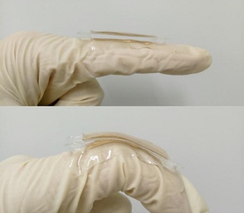
Searching for a power outlet may soon become a thing of the past.
Instead, devices will receive electricity from a small metallic tab that, when attached to the body, is capable of generating electricity from bending a finger and other simple movements.
That's the idea behind a collaborative research project led by University at Buffalo and Institute of Semiconductors (IoP) at Chinese Academy of Science (CAS). The tab -- a triboelectric nanogenerator -- is described in a study published online Jan. 31 in the journal Nano Energy.
"No one likes being tethered to a power outlet or lugging around a portable charger. The human body is an abundant source of energy. We thought: 'Why not harness it to produce our own power?'" says lead author Qiaoqiang Gan, PhD, associate professor of electrical engineering in UB's School of Engineering and Applied Sciences.
Triboelectric charging occurs when certain materials become electrically charged after coming into contact with a different material. Most everyday static electricity is triboelectric.
Researchers have proposed numerous nanogenerators that utilize the triboelectric effect; however, most are difficult to manufacture (requiring complex lithography) or are not cost effective. The tab that the UB and CAS team are developing addresses both of those concerns.
It consists of two thin layers of gold, with polydimethylsiloxane (also called PDMS, a silicon-based polymer used in contact lenses, Silly Putty and other products) sandwiched in between.
Key to the device is that one layer of gold is stretched, causing it to crumple upon release and create what looks like a miniature mountain range. When that force is reapplied, for example from a finger bending, the motion leads to friction between the gold layers and PDMS.
"This causes electrons to flow back and forth between the gold layers. The more friction, the greater the amount of power is produced," says another lead author, Yun Xu, PhD, professor of IoP at CAS.
The study describes a small tab (1.5 centimeters long, by 1 centimeter wide). It delivered a maximum voltage of 124 volts, a maximum current of 10 microamps and a maximum power density of 0.22 millwatts per square centimeter. That's not enough to quickly charge a smartphone; however it lit 48 red LED lights simultaneously.
Co-authors of the study include Huamin Chen at IoP and CAS; and Nan Zhang, a PhD student at UB.
Because the tab is easily fabricated, Zhang is leading a team of UB undergraduates which is tasked with improving the tab's performance. The team plans to use larger pieces of gold, which when stretched and folded together are expected to deliver even more electricity.
Researchers are also working on developing a portable battery to store energy produced by the tab. They envision the system serving as a power source for various wearable and self-powered electronic devices.
Share on:


Suggested Items
Fineline Global Group Acquires IBR
04/19/2024 | PRNewswireIBR Leiterplatten GmbH & Co. KG joins the Fineline Global Group and is now an integral part of one of the leading suppliers of PCBs. Fine Line Gesellschaft für Leiterplattentechnik mbH acquired 100% shares of IBR.
SEMI Applauds U.S. Chips Act Award for Samsung Electronics Facilities to Strengthen Domestic Semiconductor Supply Chain
04/17/2024 | SEMISEMI, the industry association serving the global electronics design and manufacturing supply chain, applauded the United States Department of Commerce’s announcement of a Preliminary Memorandum of Terms for an award under the CHIPS and Science Act to support the expansion of Samsung Electronics’ presence in Texas and the company’s development and production of leading-edge chips.
Microchip Technology Expands Partnership with TSMC to Strengthen Semiconductor Manufacturing Capacity
04/08/2024 | Microchip Technology Inc.Microchip Technology announced it has expanded its partnership with TSMC, the world’s leading semiconductor foundry, to enable a specialized 40 nm manufacturing capacity at Japan Advanced Semiconductor Manufacturing, Inc. (JASM), TSMC’s majority-owned manufacturing subsidiary in Kumamoto Prefecture, Japan.
MS2 a Beneficial System for Reducing Solder Dross
04/04/2024 | I-Connect007 Editorial TeamWe recently spoke with Octavio Raygoza, sales manager for P.Kay Metal in Mexico, to discuss how P.Kay’s MS2® system for reducing solder dross is both financially and environmentally responsible. By reducing solder dross up to 85%, you nearly double the output while consuming the same amount of solder.
Hentec/RPS to Exhibit Vector Selective Soldering and Odyssey Lead Tinning Systems at IPC APEX EXPO 2024
04/04/2024 | Hentec Industries/RPS AutomationHentec Industries/RPS Automation, a leading manufacturer of selective soldering, lead tinning and solderability testing equipment, is pleased to announce it will exhibit its Vector 300 selective soldering and Odyssey 925 lead tinning systems at the upcoming IPC EXPO 2024.