


 The Right Approach: I Hear the Train A Comin'
 It’s Only Common Sense: OCCAM—the Time Is Now
 Marcy's Musings: The Growing Industry
MEMS Chips Get Metalenses
February 21, 2018 | AMERICAN INSTITUTE OF PHYSICSEstimated reading time: 2 minutes
Lens technologies have advanced across all scales, from digital cameras and high bandwidth in fiber optics to the LIGO lab instruments. Now, a new lens technology that could be produced using standard computer-chip technology is emerging and could replace the bulky layers and complex geometries of traditional curved lenses.
Flat lenses, unlike their traditional counterparts, are relatively lightweight, based on optical nanomaterials known as metasurfaces. When the subwavelength nanostructures of a metasurface form certain repeated patterns, they mimic the complex curvatures that refract light, but with less bulk and an improved ability to focus light with reduced distortion. However, most of these nanostructured devices are static, which limits their functionality.
Federico Capasso, an applied physicist at Harvard University who pioneered metalens technology, and Daniel Lopez, group leader of nanofabrication and devices at Argonne National Laboratory and an early developer of microelectromechanical systems (MEMS), brainstormed about adding motion capabilities like fast scanning and beam steering to metalenses for new applications.
Capasso and Lopez developed a device that integrates mid-infrared spectrum metalenses onto MEMS. The researchers report their findings this week in APL Photonics, from AIP Publishing.
MEMS is a circuit-based technology that incorporates microelectronics, like those found in computer chips, and includes mechanical microstructures like actuators and gears. Ubiquitous in everything from cellphones to airbags, biosensing devices, appliances and optics, MEMS are fabricated using the same techniques used for integrated circuits on typical computer chips.
"Dense integration of thousands of individually controlled lens-on-MEMS devices onto a single silicon chip would allow an unprecedented degree of control and manipulation of the optical field," Lopez Said.
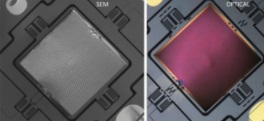
The researchers formed the metasurface lens using standard photolithography techniques on a silicon-on-insulator wafer with a 2-micron-thick top device layer, a 200-nanometer buried-oxide layer, and a 600-micron-thick handle layer. Then, they placed the flat lens onto a MEMS scanner, essentially a micromirror that deflects light for high-speed optical path length modulation. They aligned the lens with the MEMS' central platform and fixed them together by depositing small platinum patches.
"Our MEMS-integrated metasurface lens prototype can be electrically controlled to vary the angular rotation of a flat lens and can scan the focal spot by several degrees," Lopez said. "Furthermore, this proof-of-concept integration of metasurface-based flat lenses with MEMS scanners can be extended to the visible and other parts of the electromagnetic spectrum, implying the potential for application across wider fields, such as MEMS-based microscope systems, holographic and projection imaging, LIDAR (light detection and ranging) scanners and laser printing."
When electrostatically actuated, the MEMS platform controls the angle of the lens along two orthogonal axes, allowing the scanning of the flat lens focal spot by about 9 degrees in each direction. The researchers estimate that the focusing efficiency is about 85 percent.
"Such metalenses can be mass produced with the same computer-chip fabrication technology and in the future, will replace conventional lenses in a wide range of applications," Capasso said.
Share on:


Suggested Items
Koh Young Showcases Award-winning Inspection Solutions at SMTconnect with SmartRep in Hall 4A.225
04/25/2024 | Koh Young TechnologyKoh Young Technology, the industry leader in True 3D measurement-based inspection solutions, will showcase an array of award-winning inspection and measurement solutions at SMTconnect alongside its sales partner, SmartRep, in booth 4A.225 at NürnbergMesse from June 11-13, 2023. The following offers a glimpse into what Koh Young will present at the tradeshow:
Real Time with… IPC APEX EXPO 2024: Plasmatreat: Innovative Surface Preparation Solutions
04/25/2024 | Real Time with...IPC APEX EXPOIn this interview, Editor Nolan Johnson speaks with Hardev Grewal, CEO and president of Plasmatreat, a developer of atmospheric plasma solutions. Plasmatreat uses clean compressed air and electricity to create plasma, offering environmentally friendly methods for surface preparation. Their technology measures plasma density for process optimization and can remove organic micro-contamination. Nolan and Hardev also discuss REDOX-Tool, a new technology for removing metal oxides.
Nanotechnology Market to Surpass $53.51 Billion by 2031
04/25/2024 | PRNewswireSkyQuest projects that the nanotechnology market will attain a value of USD 53.51 billion by 2031, with a CAGR of 36.4% over the forecast period (2024-2031).
Cadence, TSMC Collaborate on Wide-Ranging Innovations to Transform System and Semiconductor Design
04/25/2024 | Cadence Design SystemsCadence Design Systems, Inc. and TSMC have extended their longstanding collaboration by announcing a broad range of innovative technology advancements to accelerate design, including developments ranging from 3D-IC and advanced process nodes to design IP and photonics.
SMC Korea 2024 to Highlight Semiconductor Materials Trends and Innovations on Industry’s Path to $1 Trillion
04/24/2024 | SEMIWith Korea a major consumer of semiconductor materials and advanced materials a key driver of innovation on the industry’s path to $1 trillion, industry leaders and experts will gather at SMC (Strategic Materials Conference) Korea 2024 on May 29 at the Suwon Convention Center in Gyeonggi-do, South Korea to provide insights into the latest materials developments and trends. Registration is open.