


 It’s Only Common Sense: OCCAM—the Time Is Now
 Marcy's Musings: The Growing Industry
 Dan’s Biz Bookshelf: Seeing the How
Reinventing the Inductor
February 22, 2018 | University of California - Santa BarbaraEstimated reading time: 3 minutes
A basic building block of modern technology, inductors are everywhere: cellphones, laptops, radios, televisions, cars. And surprisingly, they are essentially the same today as in 1831, when they were first created by English scientist Michael Faraday.
The particularly large size of inductors made according to Faraday’s design are a limiting factor in delivering the miniaturized devices that will help realize the potential of the Internet of Things, which promises to connect people to some 50 billion objects by 2020. That lofty goal is expected to have an estimated economic impact between $2.7 and $6.2 trillion annually by 2025.
Now, a team at UC Santa Barbara, led by Kaustav Banerjee, a professor in the Department of Electrical and Computer Engineering, has taken a materials-based approach to reinventing this fundamental component of modern electronics. The findings appear in the journal Nature Electronics.
Banerjee and his UCSB team — lead author Jiahao Kang, Junkai Jiang, Xuejun Xie, Jae Hwan Chu and Wei Liu, all members of his Nanoelectronics Research Lab — worked with colleagues from Shibaura Institute of Technology in Japan and Shanghai Jiao Tong University in China to exploit the phenomenon of kinetic inductance to demonstrate a fundamentally different kind of inductor.
All inductors generate both magnetic and kinetic inductance, but in typical metal conductors, the kinetic inductance is so small as to be unnoticeable. “The theory of kinetic inductance has long been known in condensed-matter physics, but nobody ever used it for inductors, because in conventional metallic conductors, kinetic inductance is negligible,” Banerjee explained.
Unlike magnetic inductance, kinetic inductance does not depend on the surface area of the inductor. Rather, kinetic inductance resists current fluctuations that alter the velocity of the electrons, and the electrons resist such change according to Newton’s law of inertia.
Historically, as the technology of transistors and interconnects that link them has advanced, the elements have become smaller. But the inductor, which in its simplest form is a metallic coil wound around a core material, has been the exception.
“On-chip inductors based on magnetic inductance cannot be made smaller in the same way transistors or interconnects scale, because you need a certain amount of surface area to get a certain magnetic flux or inductance value,” explained lead author Kang, who recently completed his Ph.D. under Banerjee’s supervision.
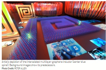
The UCSB team designed a new kind of spiral inductor comprised of multiple layers of graphene. Single-layer graphene exhibits a linear electronic band structure and a correspondingly large momentum relaxation time (MRT) — a few picoseconds or higher compared to that of conventional metallic conductors (like copper used in traditional on-chip inductors), which ranges from 1/1000 to 1/100 of a picosecond. But single-layer graphene has too much resistance for application on an inductor.
However, multilayer graphene offers a partial solution by providing lower resistance, but interlayer couplings cause its MRT to be insufficiently small. The researchers overcame that dilemma with a unique solution: They chemically inserted bromine atoms between the graphene layers — a process called intercalation — that not only further reduced resistance but also separated the graphene layers just enough to essentially decouple them, extending the MRT and thereby increasing kinetic inductance.
The revolutionary inductor, which works in the 10-50 GHz range, offers one-and-a-half times the inductance density of a traditional inductor, leading to a one-third reduction in area while also providing extremely high efficiency. Previously, high inductance and reduced size had been an elusive combination.
“There is plenty of room to increase the inductance density further by increasing the efficiency of the intercalation process, which we are now exploring,” said co-author Jiang.
“We essentially engineered a new nanomaterial to bring forward the previously ‘hidden physics’ of kinetic inductance at room temperature and in a range of operating frequencies targeted for next-generation wireless communications,” Banerjee added.
While Faraday’s version of the inductor proved crucial for practical large scale use of electricity for power and telegraph communication, Banerjee’s version could pave the way for next-generation communications, sensing and energy storage for smarter living.
Share on:


Suggested Items
Designer’s Notebook: What Designers Need to Know About Manufacturing, Part 2
04/24/2024 | Vern Solberg -- Column: Designer's NotebookThe printed circuit board (PCB) is the primary base element for providing the interconnect platform for mounting and electrically joining electronic components. When assessing PCB design complexity, first consider the component area and board area ratio. If the surface area for the component interface is restricted, it may justify adopting multilayer or multilayer sequential buildup (SBU) PCB fabrication to enable a more efficient sub-surface circuit interconnect.
Insulectro’s 'Storekeepers' Extend Their Welcome to Technology Village at IPC APEX EXPO
04/03/2024 | InsulectroInsulectro, the largest distributor of materials for use in the manufacture of PCBs and printed electronics, welcomes attendees to its TECHNOLOGY VILLAGE during this year’s IPC APEX EXPO at the Anaheim Convention Center, April 9-11, 2024.
ENNOVI Introduces a New Flexible Circuit Production Process for Low Voltage Connectivity in EV Battery Cell Contacting Systems
04/03/2024 | PRNewswireENNOVI, a mobility electrification solutions partner, introduces a more advanced and sustainable way of producing flexible circuits for low voltage signals in electric vehicle (EV) battery cell contacting systems.
Heavy Copper PCBs: Bridging the Gap Between Design and Fabrication, Part 1
04/01/2024 | Yash Sutariya, Saturn Electronics ServicesThey call me Sparky. This is due to my talent for getting shocked by a variety of voltages and because I cannot seem to keep my hands out of power control cabinets. While I do not have the time to throw the knife switch to the off position, that doesn’t stop me from sticking screwdrivers into the fuse boxes. In all honesty, I’m lucky to be alive. Fortunately, I also have a talent for building high-voltage heavy copper circuit boards. Since this is where I spend most of my time, I can guide you through some potential design for manufacturability (DFM) hazards you may encounter with heavy copper design.
Trouble in Your Tank: Supporting IC Substrates and Advanced Packaging, Part 5
03/19/2024 | Michael Carano -- Column: Trouble in Your TankDirect metallization systems based on conductive graphite or carbon dispersion are quickly gaining acceptance worldwide. Indeed, the environmental and productivity gains one can achieve with these processes are outstanding. In today’s highly competitive and litigious environment, direct metallization reduces costs associated with compliance, waste treatment, and legal issues related to chemical exposure. What makes these processes leaders in the direct metallization space?