


 The Right Approach: I Hear the Train A Comin'
 It’s Only Common Sense: OCCAM—the Time Is Now
 Marcy's Musings: The Growing Industry
A Marriage of Light-Manipulation Technologies
February 28, 2018 | Argonne National LaboratoryEstimated reading time: 3 minutes
Researchers have, for the first time, integrated two technologies widely used in applications such as optical communications, bio-imaging and Light Detection and Ranging (LIDAR) systems that scan the surroundings of self-driving cars and trucks.
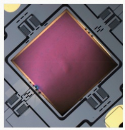
Image caption: This image gives a close-up view of a metasurface-based flat lens (square piece) integrated onto a MEMS scanner. Integration of MEMS devices with metalenses will help manipulate light in sensors by combining the strengths of high-speed dynamic control and precise spatial manipulation of wave fronts. This image was taken with an optical microscope at Argonne’s Center for Nanoscale Materials.
In the collaborative effort between the U.S. Department of Energy’s (DOE) Argonne National Laboratory and Harvard University, researchers successfully crafted a metasurface-based lens atop a Micro-Electro-Mechanical System (MEMS) platform. The result is a new infrared light-focusing system that combines the best features of both technologies while reducing the size of the optical system.
Metasurfaces can be structured at the nanoscale to work like lenses. These metalenses were pioneered by Federico Capasso, Harvard’s Robert L. Wallace Professor of Applied Physics, and his group at the Harvard John A. Paulson School of Engineering and Applied Sciences (SEAS). The lenses are rapidly finding applications because they are much thinner and less bulky than existing lenses, and can be made with the same technology used to fabricate computer chips. The MEMSs, meanwhile, are small mechanical devices that consist of tiny, movable mirrors.
“These devices are key today for many technologies. They have become technologically pervasive and have been adopted for everything from activating automobile air bags to the global positioning systems of smart phones,” said Daniel Lopez, Nanofabrication and Devices Group Leader at Argonne’s Center for Nanoscale Materials, a DOE Office of Science User Facility.
Lopez, Capasso and four co-authors describe how they fabricated and tested their new device in an article in APL Photonics, titled “Dynamic metasurface lens based on MEMS technology.” The device measures 900 microns in diameter and 10 microns in thickness (a human hair is approximately 50 microns thick).
The collaboration’s ongoing work to further develop novel applications for the two technologies is conducted at Argonne’s Center for Nanoscale Materials, SEAS and the Harvard Center for Nanoscale Systems, which is part of the National Nanotechnology Coordinated Infrastructure.
In the technologically merged optical system, MEMS mirrors reflect scanned light, which the metalens then focuses without the need for an additional optical component such as a focusing lens. The challenge that the Argonne/Harvard team overcame was to integrate the two technologies without hurting their performance.
The eventual goal would be to fabricate all components of an optical system — the MEMS, the light source and the metasurface-based optics — with the same technology used to manufacture electronics today.
“Then, in principle, optical systems could be made as thin as credit cards,” Lopez said.
These lens-on-MEMS devices could advance the LIDAR systems used to guide self-driving cars. Current LIDAR systems, which scan for obstacles in their immediate proximity, are, by contrast, several feet in diameter.
“You need specific, big, bulky lenses, and you need mechanical objects to move them around, which is slow and expensive,” said Lopez.
“This first successful integration of metalenses and MEMS, made possible by their highly compatible technologies, will bring high speed and agility to optical systems, as well unprecedented functionalities,” said Capasso.
This work was also supported by the Air Force Office of Scientific Research, the National Science Foundation and the Singapore Agency for Science, Technology and Research’s National Science Scholarship.
About Argonne National Laboratory
Argonne National Laboratory seeks solutions to pressing national problems in science and technology. The nation's first national laboratory, Argonne conducts leading-edge basic and applied scientific research in virtually every scientific discipline. Argonne researchers work closely with researchers from hundreds of companies, universities, and federal, state and municipal agencies to help them solve their specific problems, advance America's scientific leadership and prepare the nation for a better future. With employees from more than 60 nations, Argonne is managed by UChicago Argonne, LLC for the U.S. Department of Energy's Office of Science.
About U.S. Department of Energy's Office of Science
The U.S. Department of Energy's Office of Science is the single largest supporter of basic research in the physical sciences in the United States and is working to address some of the most pressing challenges of our time.
Share on:


Suggested Items
Lockheed Martin Successfully Transitions Long Range Discrimination Radar To The Missile Defense Agency
04/23/2024 | Lockheed MartinThe Long Range Discrimination Radar (LRDR) at Clear Space Force Station in Clear, Alaska, completed DD250 final acceptance and was officially handed over to the Missile Defense Agency in preparation for an Operational Capability Baseline (OCB) decision and final transition to the Warfighter. In addition, prior to this transition, the system has started Space Domain Awareness data collects for the United States Space Force.
Real Time with... IPC APEX EXPO 2024: AI Implementation at Omron
04/18/2024 | Real Time with...IPC APEX EXPOEditor Nolan Johnson and Omron Product Manager Nick Fieldhouse discuss the company's focus on AI implementation to enhance customer experience and results. They address programming challenges and how AI can help customers achieve better outcomes with less experience. Omron's AI is compatible with existing systems, facilitating easy upgrades.
Cadence Unveils Palladium Z3 and Protium X3 Systems
04/18/2024 | Cadence Design SystemsThe Palladium Z3 and Protium X3 systems offer increased capacity, and scale from job sizes of 16 million gates up to 48 billion gates, so the largest SoCs can be tested as a whole rather than just partial models, ensuring proper functionality and performance.
Australian Flow Batteries and The SCHMID Group Announce Groundbreaking Memorandum of Understanding
04/17/2024 | SCHMID GroupAustralian Flow Batteries Pty Ltd (AFB), a leader in innovative energy solutions and economical, safe, and reliable power storage, and SCHMID Energy Systems GmbH a company of the German SCHMID Group, a global technology leader with a rich history in delivering innovative solutions across multiple industries including Electronics, Renewables, and Energy Storage sectors, are thrilled to announce the signing of a Memorandum of Understanding (MoU)
Ansys Joins BAE Systems’ Mission Advantage Program to Advance Digital Engineering Across US Department of Defense
04/16/2024 | ANSYSAnsys announced it is working with BAE Systems, Inc., to accelerate the adoption of digital engineering and MBSE across the Department of Defense (DoD).