


 The Right Approach: I Hear the Train A Comin'
 It’s Only Common Sense: OCCAM—the Time Is Now
 Marcy's Musings: The Growing Industry
Femtosecond Laser Fabrication: Realizing Dynamics Control of Electrons
March 27, 2018 | Changchun Institute of Optics, Fine Mechanics and PhysicsEstimated reading time: 1 minute
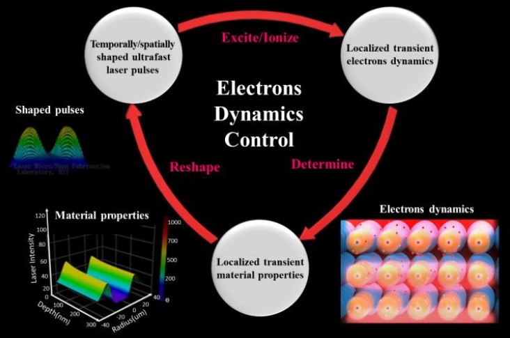
Femtosecond lasers are capable of processing any solid material with high quality and high precision using their ultrafast and ultra-intense characteristics. With the continuous development of laser technology, ultrafast laser manufacturing would hopefully become one of the primary methods employed in high-end manufacturing in the future.
Recently, researchers realized a new method termed electrons dynamics control for ultrafast laser micro/nano fabrication. For the first time, the localized transient electrons dynamics in laser fabrication can be actively controlled to manipulate material properties, which greatly enhances the efficiency, quality, uniformity, and precision of laser fabrication.
This research is conducted by the group of Professor Lan Jiang from Beijing Institute of Technology, in cooperation with Professor Tian-Hong Cui from Minnesota University, Twin City, and Professor Yongfeng Lu from Nebraska University, Lincoln. Their research results were recently reviewed in Light: Science and Applications.
Over the past decade, the research group has devoted their efforts to studying novel methods of manufacturing based on electrons dynamics control. They used the temporally/spatially shaped ultrafast laser to control the localized transient electron dynamics (e.g., density, temperature, and distribution); furthermore, they modified the localized transient material properties and adjusted material phase change; eventually, they implemented the novel fabrication method.
They established a multiscale model of ultrafast laser materials interactions and predicted that the temporally/spatially shaped ultrafast pulses can control the laser material interaction processes. Furthermore, on the basis of the theoretical predictions, they experimentally verified the validity of the electrons dynamics control method. In addition, they proposed and implemented a multiscale measurement system for observing femtosecond laser ablation dynamics from femtosecond scale to second scale, which provided experimental evidences for the proposed mechanism.
Using this method, they greatly improved fabrication efficiency, quality, repeatability, and precision, as well as extended the fabrication limits of laser manufacturing. The new method has resolved some critical manufacturing challenges and already been applied to a series of major Chinese national projects.
This novel method has realized the active control of localized transient electrons dynamics in the laser fabrication process for the first time. Furthermore, it has opened the wide exciting possibilities in the control of fabrication on electron level, which may provide revolutionary contributions to high-end manufacturing, material properties manipulation, and chemical reactions control.
Share on:


Suggested Items
Real Time with… IPC APEX EXPO 2024: Tools, Training, and Trends in Manufacturing Engineering
04/25/2024 | Real Time with...IPC APEX EXPOGuest Editor Kelly Dack and Product Specialist Erik Bateham of Polar Instruments discuss Polar's latest technology, including their role in aiding manufacturing engineers. They highlight the advanced capabilities of Polar's tools and the critical role of signal integrity analysis, as well as the importance of accurate modeling in board manufacturing. Polar's unique training approach and demonstration contact details are also explored.
TTM Celebrates the Grand Opening of Its First Manufacturing Facility in Penang
04/25/2024 | TTM Technologies, Inc.TTM Technologies, Inc., a leading global manufacturer of technology solutions including mission systems, radio frequency (RF) components and RF microwave/microelectronic assemblies, and quick-turn and technologically advanced printed circuit boards (PCBs), officially opened its first manufacturing plant in Penang, Malaysia with an investment of USD200 million (approximately RM958 million).
Listen Up! The Intricacies of PCB Drilling Detailed in New Podcast Episode
04/25/2024 | I-Connect007In episode 5 of the podcast series, On the Line With: Designing for Reality, Nolan Johnson and Matt Stevenson continue down the manufacturing process, this time focusing on the post-lamination drilling process for PCBs. Matt and Nolan delve into the intricacies of the PCB drilling process, highlighting the importance of hole quality, drill parameters, and design optimization to ensure smooth manufacturing. The conversation covers topics such as drill bit sizes, aspect ratios, vias, challenges in drilling, and ways to enhance efficiency in the drilling department.
Elevating PCB Design Engineering With IPC Programs
04/24/2024 | Cory Blaylock, IPCIn a monumental stride for the electronics manufacturing industry, IPC has successfully championed the recognition of the PCB Design Engineer as an official occupation by the U.S. Department of Labor (DOL). This pivotal achievement not only underscores the critical role of PCB design engineers within the technology landscape, but also marks the beginning of a transformative journey toward nurturing a robust, skilled workforce ready to propel our industry into the future.
Fujitsu, METRON Collaborate to Drive ESG Success
04/24/2024 | JCN NewswireFujitsu Limited and METRON SAS, a French cleantech company specializing in energy management solutions for industrial decarbonization, today announced a strategic initiative to contribute to the realization of carbon neutrality in the manufacturing industry.