


 The Right Approach: I Hear the Train A Comin'
 It’s Only Common Sense: OCCAM—the Time Is Now
 Marcy's Musings: The Growing Industry
Atomically Thin Light Emitting Device Opens the Possibility for 'Invisible' Displays
March 27, 2018 | Berkeley LabEstimated reading time: 2 minutes
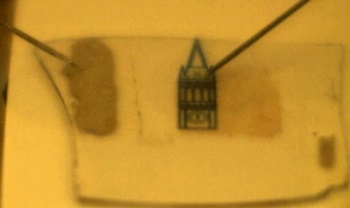
UC Berkeley engineers have built a bright-light emitting device that is millimeters wide and fully transparent when turned off. The light emitting material in this device is a monolayer semiconductor, which is just three atoms thick.
The device opens the door to invisible displays on walls and windows – displays that would be bright when turned on but see-through when turned off — or in futuristic applications such as light-emitting tattoos, according to the researchers.
“The materials are so thin and flexible that the device can be made transparent and can conform to curved surfaces,” said Der-Hsien Lien, a postdoctoral fellow at UC Berkeley and a co-first author along with Matin Amani and Sujay Desai, both doctoral students in the Department of Electrical Engineering and Computer Sciences at Berkeley.
The device was developed in the laboratory of Ali Javey, professor of Electrical Engineering and Computer Sciences at Berkeley. In 2015, Javey’s lab published research in the journal Science showing that monolayer semiconductors are capable of emitting bright light, but stopped short of building a light-emitting device. The new work in Nature Communications overcame fundamental barriers in utilizing LED technology on monolayer semiconductors, allowing for such devices to be scaled from sizes smaller than the width of a human hair up to several millimeters. That means that researchers can keep the thickness small, but make the lateral dimensions (width and length) large, so that the light intensity can be high.
Commercial LEDs consist of a semiconductor material that is electrically injected with positive and negative charges, which produce light when they meet. Typically, two contact points are used in a semiconductor-based light emitting device; one for injecting negatively charged particles and one injecting positively charged particles. Making contacts that can efficiently inject these charges is a fundamental challenge for LEDs, and it is particularly challenging for monolayer semiconductors since there is so little material to work with.
The Berkeley research team engineered a way to circumvent this challenge by designing a new device that only requires one contact on the semiconductor. By laying the semiconductor monolayer on an insulator and placing electrodes on the monolayer and underneath the insulator, the researchers could apply an AC signal across the insulator. During the moment when the AC signal switches its polarity from positive to negative (and vice versa), both positive and negative charges are present at the same time in the semiconductor, creating light.
The researchers showed that this mechanism works in four different monolayer materials, all of which emit different colors of light.
This device is a proof-of-concept, and much research still remains, primarily to improve efficiency. Measuring this device’s efficiency is not straightforward, but the researchers think it’s about 1 percent efficient. Commercial LEDs have efficiencies of around 25 to 30 percent.
The concept may be applicable to other devices and other kinds of materials, the device could one day have applications in a number of fields where having invisible displays are warranted. That could be an atomically thin display that’s imprinted on a wall or even on human skin.
“A lot of work remains to be done and a number of challenges need to be overcome to further advance the technology for practical applications,” Javey said. “However, this is one step forward by presenting a device architecture for easy injection of both charges into monolayer semiconductors.”
Share on:


Suggested Items
D Coupon Testing and Data Insights With GreenSource Fabrication
04/17/2024 | Marcy LaRont, PCB007 MagazineMarcy LaRont spoke with Steve Karas of GreenSource Fabrication at the SMTA UHDI conference in March. He presented a case study that GreenSource undertook with a customer on critical via reliability with advanced materials and used the experience to highlight the importance and effectiveness of D coupon testing. He also discussed GreenSource’s approach to data aggregation and a new system they developed to use collected data effectively.
Real Time with... IPC APEX EXPO 2024: Exploring Silicone Solutions with R&D Director of CHT
04/17/2024 | Real Time with...IPC APEX EXPOIn this interview, Gerry Ellis, the R&D director for CHT, discusses the product range offered by his company. He explains the challenges in creating base formulations, the drive to make products more user-friendly, and the various application techniques involved. Ellis also highlights the key market segments and the significance of providing efficient solutions to customers.
The World of Electronics and Standards: A Conversation with Frank Honyotski, STI
04/03/2024 | Marcy LaRont, PCB007 MagazineMarcy LaRont of I-Connect007 speaks with Frank Honyotski of STI Electronics, who discusses the services offered by STI, including training, engineering, and failure analysis. He highlights his involvement with IPC standards development and emphasizes the importance of industry professionals engaging in standards development.
Demand Rebounds, Global LED Industry Revenue Expected to Grow 3% in 2024 with Market Focus on Automotive Displays
04/01/2024 | TrendForceTrendForce’s latest LED industry report indicates that the global market is set to recover in 2024, with estimated revenues reaching US$13 billion—marking a YoY growth of 3%.
Orbex Secures Patent for 'Petal Fold' Reusable Rocket Technology
03/29/2024 | OrbexOrbex has successfully patented its REFLIGHT reusable rocket technology following patent approval in several European markets, based on the patent grant by the European Patent Office, as well as in the United States.