


 It’s Only Common Sense: OCCAM—the Time Is Now
 Marcy's Musings: The Growing Industry
 Dan’s Biz Bookshelf: Seeing the How
A New Way to Atomically Thin Materials
April 5, 2018 | WileyEstimated reading time: 2 minutes
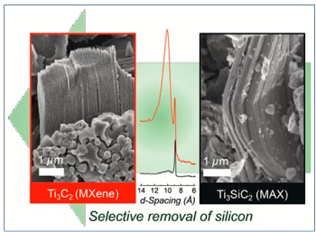
Metallic conductivity and hydrophilicity of MXenes have established them as electrodes in rechargeable batteries and supercapacitors, as well as other applications, including photothermal cancer therapy, electromagnetic shielding, water purification and gas sensing. In the journal Angewandte Chemie, researchers have now introduced a new production method. Instead of using conventional, yet more expensive, titanium aluminum carbide, they selectively etch silicon out of titanium silicon carbide, a cheaper and more common precursor, to synthesize titanium carbide.
Two-dimensional materials, consisting of extremely thin layers that are a few atoms thick, have unique properties that are completely different than the normal three-dimensional versions. A prominent example of this is graphene, which is made of single layers of carbon atoms. In 2011, a new class of two-dimensional materials was synthesized at Drexel University in Philadelphia (Pennsylvania, USA). Known as MXenes, the materials are made of transition metal carbides and nitrides, where the M stands for a transition metal, such as titanium, vanadium, or molybdenum, X can be carbon and/or nitrogen, and many compositions are available (about 30 have already been experimentally demonstrated and dozens more are expected). One such MXene is titanium carbide, Ti3C2.
Obtaining the desired MXene usually involves a roundabout process: Layered carbides and nitrides, known as MAX phases, are selectively etched with hydrofluoric acid to remove the layers of the “A” element, which is a group 13 or 14 element such as aluminum, silicon, or germanium. In this way, titanium carbide can be obtained by etching the aluminum out of titanium aluminum carbide (Ti3AlC2). However, this starting material is expensive, and the production is complex. In contrast, the silicon analog, titanium silicon carbide (Ti3SiC2), is commercially available and less expensive. Ti3SiC2 was the first MAX phase Drexel researchers tried to selectively etch in 2011, but synthesis failed using hydrofluoric acid alone because the silicon atoms are strongly bound to the adjacent transition metal atoms.
A team led by Yury Gogotsi at Drexel University has now developed a successful variation of this process. By adding an oxidizing agent, the researchers could weaken the silicon bonds and oxidize silicon. Using mixtures of hydrofluoric acid and an oxidizing agent like nitric acid, hydrogen peroxide, or potassium permanganate, the team produced titanium carbide MXene by selectively removing silicon out of Ti3SiC2.
The etching process leaves behind stacks of titanium carbide, which can be delaminated to make flakes, which are approximately 1 nanometer in thickness. The researchers used this method to make flexible, electrically conducting titanium carbide films on a relatively large scale.
This new method could make the production of MXenes easier, and open pathways to the production of new MXenes and related two-dimensional materials from silicon-containing precursors, expanding the family of 2D nanosheets available to scientists and engineers.
Share on:


Suggested Items
SMC Korea 2024 to Highlight Semiconductor Materials Trends and Innovations on Industry’s Path to $1 Trillion
04/24/2024 | SEMIWith Korea a major consumer of semiconductor materials and advanced materials a key driver of innovation on the industry’s path to $1 trillion, industry leaders and experts will gather at SMC (Strategic Materials Conference) Korea 2024 on May 29 at the Suwon Convention Center in Gyeonggi-do, South Korea to provide insights into the latest materials developments and trends. Registration is open.
Groundbreaking Ceremony Marks the Beginning of a New Era for Newccess Industrial; The Construction of the MINGXIN Building
04/12/2024 | Newccess IndustrialOn a clear and sunny day in March, the groundbreaking ceremony for the MINGXIN Building took place in Shenzhen, China. This moment marked the official commencement of construction for a project that will reshape the semiconductor materials industry.
The Need for a Holistic Global Sustainability Standard
04/10/2024 | Michael Ford, Aegis SoftwareNo one can deny that the resources of our fragile planet are finite. The environment seems like a third party, subject to constant degradation. We’re acutely aware of the effects of pollution on our climate, and despite our “throw-away” culture, recycling and recovery of materials has remained relatively expensive, even as we use more energy just to survive.
iNEMI Publishes Four Roadmap Topics
04/04/2024 | iNEMIThe International Electronics Manufacturing Initiative (iNEMI) announces the availability of the first roadmap topics in the new iNEMI Roadmap format. Printed circuit boards, sustainable electronics, smart manufacturing, and mmWave materials and test are now available online.
Insulectro’s 'Storekeepers' Extend Their Welcome to Technology Village at IPC APEX EXPO
04/03/2024 | InsulectroInsulectro, the largest distributor of materials for use in the manufacture of PCBs and printed electronics, welcomes attendees to its TECHNOLOGY VILLAGE during this year’s IPC APEX EXPO at the Anaheim Convention Center, April 9-11, 2024.