


 It’s Only Common Sense: OCCAM—the Time Is Now
 Marcy's Musings: The Growing Industry
 Dan’s Biz Bookshelf: Seeing the How
EU Project ESPResSo to Make Perovskite Solar Cells a Market Reality
April 20, 2018 | ImecEstimated reading time: 3 minutes
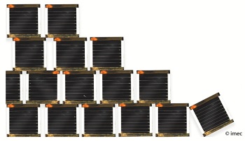
Imec, a partner in EnergyVille, has been named the coordinator of an ambitious three-year European Union (EU) funded project, “ESPResSo” (Efficient Structures and Processes for Reliable Perovskite Solar Modules), that gathers known leaders in the field of perovskite PV technology to revolutionize Europe’s photovoltaics (PV) industry.
The ESPResSo consortium has been granted over 5M euro by the European Union to overcome the limitations of today’s state-of-the-art perovskite PV technology, bring perovskite solar cells to the next maturity level, and demonstrate their practical application. The members of the consortium include the fundamental research organizations Ecole Polytechnique Federale de Lausanne (EPFL), Switzerland and Consiglio Nazionale delle Ricerche (CNR), Italy; perovskite solar cell scale-up and industrialization members imec, Belgium, Universita degli Studi di Roma Tor Vergata (UNITOV-CHOSE), Italy and Fraunhofer Institute for Solar Energy Systems ISE, Germany; and experts in sustainability and renewable energies CSGI (Consorzio Interuniversitario per lo Sviluppo dei Sistemi a Grande Interfase), Italy and University of Cyprus, Cyprus. Members representing materials development include Dycotec Materials LTD, United Kingdom, Dyenamo AB, Sweden and Corning SAS, France; equipment manufacturer, M-Solv LTD, United Kingdom; along with perovskite solar cell technology developers Saule Technologies, Poland, and building-integrated photovoltaics developer, Onyx Solar Energy SL, Spain.
With its low-cost materials and low temperature deposition processes, perovskite-based PV technology has the potential to takes its place in the thin-film PV market. Perovskite solar cells have already demonstrated high efficiencies (above 22%) that rival those of established mainstream thin-film PV technologies like copper-indium-gallium-selenide (CIGS) and cadmium-telluride (CdTe). The challenge is now to transfer the unprecedented progress that the perovskite PV cell technology has made in recent years from its cell level into a scalable, stable, low-cost technology on module level.
“Every aspect of our lives – from our homes to our workplaces, hospitals, schools and farms - depends on the nonstop availability of energy,” stated Tom Aernouts, imec group leader of thin-film photovoltaics and researcher at EnergyVille. “Perovskite cells demonstrate clear potential to support world’s energy demands cost-effectively. The ultimate aim of the partners of the ESPResSo project is to achieve this by bringing perovskite photovoltaics from the lab to the fab.”
The ESPResSo team targets alternative cost effective materials, novel cell concepts and architectures, and advanced processing know-how and equipment to overcome the current limitations of this technology. The consortium aims to bring the cell performance close to its theoretical limit by demonstrating cell efficiency of more than 24% (on 1cm²) and less than 10% degradation in cell efficiency following thermal stress at 85°C, 85% RH for over 1000h. Scale up activities utilising solution processed slot-die coating and laser processing will additionally deliver modules with more than 17% efficiency showing long-term (>20 years) reliable performance as deduced from IEC-compliant test conditions.
The ESPResSo team also envisions integrating modules in façade elements demonstrating a levelised cost of electricity (LCoE) of ≤ 0.05€/kWh. Prototyping advanced, arbitrary-shaped architectures with specific materials and process combinations will emphasize that new highly innovative applications like on flexible substrates or with high semi-transparency are well accessible in the mid- to longer-term with this very promising thin-film PV technology.
About imec
Imec is the world-leading research and innovation hub in nanoelectronics, energy and digital technologies. The combination of our widely acclaimed leadership in microchip technology, profound software and ICT expertise is what makes us unique. By leveraging our world-class infrastructure and local and global ecosystem of partners across a multitude of industries, we create groundbreaking innovation in application domains such as healthcare, smart cities and mobility, logistics and manufacturing, energy, and education.
As a trusted partner for companies, start-ups and universities, we bring together close to 3,500 brilliant minds from over 70 nationalities. Imec is headquartered in Leuven, Belgium, and has distributed R&D groups at a number of Flemish universities, in the Netherlands, Taiwan, USA, China, and offices in India and Japan. In 2016, imec’s revenue (P&L) totaled 496 million euro.
Share on:


Suggested Items
Designer’s Notebook: What Designers Need to Know About Manufacturing, Part 2
04/24/2024 | Vern Solberg -- Column: Designer's NotebookThe printed circuit board (PCB) is the primary base element for providing the interconnect platform for mounting and electrically joining electronic components. When assessing PCB design complexity, first consider the component area and board area ratio. If the surface area for the component interface is restricted, it may justify adopting multilayer or multilayer sequential buildup (SBU) PCB fabrication to enable a more efficient sub-surface circuit interconnect.
Insulectro’s 'Storekeepers' Extend Their Welcome to Technology Village at IPC APEX EXPO
04/03/2024 | InsulectroInsulectro, the largest distributor of materials for use in the manufacture of PCBs and printed electronics, welcomes attendees to its TECHNOLOGY VILLAGE during this year’s IPC APEX EXPO at the Anaheim Convention Center, April 9-11, 2024.
ENNOVI Introduces a New Flexible Circuit Production Process for Low Voltage Connectivity in EV Battery Cell Contacting Systems
04/03/2024 | PRNewswireENNOVI, a mobility electrification solutions partner, introduces a more advanced and sustainable way of producing flexible circuits for low voltage signals in electric vehicle (EV) battery cell contacting systems.
Heavy Copper PCBs: Bridging the Gap Between Design and Fabrication, Part 1
04/01/2024 | Yash Sutariya, Saturn Electronics ServicesThey call me Sparky. This is due to my talent for getting shocked by a variety of voltages and because I cannot seem to keep my hands out of power control cabinets. While I do not have the time to throw the knife switch to the off position, that doesn’t stop me from sticking screwdrivers into the fuse boxes. In all honesty, I’m lucky to be alive. Fortunately, I also have a talent for building high-voltage heavy copper circuit boards. Since this is where I spend most of my time, I can guide you through some potential design for manufacturability (DFM) hazards you may encounter with heavy copper design.
Trouble in Your Tank: Supporting IC Substrates and Advanced Packaging, Part 5
03/19/2024 | Michael Carano -- Column: Trouble in Your TankDirect metallization systems based on conductive graphite or carbon dispersion are quickly gaining acceptance worldwide. Indeed, the environmental and productivity gains one can achieve with these processes are outstanding. In today’s highly competitive and litigious environment, direct metallization reduces costs associated with compliance, waste treatment, and legal issues related to chemical exposure. What makes these processes leaders in the direct metallization space?