


 Marcy's Musings: The Growing Industry
 It’s Only Common Sense: Here’s What To Do After IPC APEX EXPO 2024
 Dan’s Biz Bookshelf: Seeing the How
Atomically Thin Magnetic Device Could Lead to New Memory Technologies
May 4, 2018 | University of WashingtonEstimated reading time: 3 minutes
Magnetic materials are the backbone of modern digital information technologies, such as hard-disk storage. A University of Washington-led team has now taken this one step further by encoding information using magnets that are just a few layers of atoms in thickness. This breakthrough may revolutionize both cloud computing technologies and consumer electronics by enabling data storage at a greater density and improved energy efficiency.
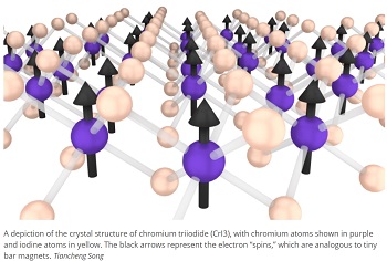
In a study published online May 3 in the journal Science, the researchers report that they used stacks of ultrathin materials to exert unprecedented control over the flow of electrons based on the direction of their spins — where the electron “spins” are analogous to tiny, subatomic magnets. The materials that they used include sheets of chromium tri-iodide (CrI3), a material described in 2017 as the first ever 2-D magnetic insulator. Four sheets — each only atoms thick — created the thinnest system yet that can block electrons based on their spins while exerting more than 10 times stronger control than other methods.
“Our work reveals the possibility to push information storage based on magnetic technologies to the atomically thin limit,” said co-lead author Tiancheng Song, a UW doctoral student in physics.
In related research, published April 23 in Nature Nanotechnology, the team found ways to electrically control the magnetic properties of this atomically thin magnet.
“With the explosive growth of information, the challenge is how to increase the density of data storage while reducing operation energy,” said corresponding author Xiaodong Xu, a UW professor of physics and of materials science and engineering, and faculty researcher at the UW Clean Energy Institute. “The combination of both works points to the possibility of engineering atomically thin magnetic memory devices with energy consumption orders of magnitude smaller than what is currently achievable.”
The new Science paper also looks at how this material could allow for a new type of memory storage that exploits the electron spins in each individual sheet.
The researchers sandwiched two layers of CrI3 between conducting sheets of graphene. They showed that, depending on how the spins are aligned between each of the CrI3 sheets, the electrons can either flow unimpeded between the two graphene sheets or were largely blocked from flowing. These two different configurations could act as the bits — the zeroes and ones of binary code in everyday computing — to encode information.
“The functional units of this type of memory are magnetic tunnel junctions, or MTJ, which are magnetic ‘gates’ that can suppress or let through electrical current depending on how the spins align in the junction,” said co-lead author Xinghan Cai, a UW postdoctoral researcher in physics. “Such a gate is central to realizing this type of small-scale data storage.”
With up to four layers of CrI3, the team discovered the potential for “multi-bit” information storage. In two layers of CrI3, the spins between each layer are either aligned in the same direction or opposite directions, leading to two different rates that the electrons can flow through the magnetic gate. But with three and four layers, there are more combinations for spins between each layer, leading to multiple, distinct rates at which the electrons can flow through the magnetic material from one graphene sheet to the other.
“Instead of your computer having just two choices to store a piece of data in, it can have a choice A, B, C, even D and beyond,” said co-author Bevin Huang, a UW doctoral student in physics. “So not only would storage devices using CrI3 junctions be more efficient, but they would intrinsically store more data.”
The researchers’ materials and approach represent a significant improvement over existing techniques under similar operating conditions using magnesium oxide, which is thicker, less effective at blocking electrons and lacks the option for multi-bit information storage.
“Although our current device requires modest magnetic fields and is only functional at low temperature, infeasible for use in current technologies, the device concept and operational principle are novel and groundbreaking,” said Xu. “We hope that with developed electrical control of magnetism and some ingenuity, these tunnel junctions can operate with reduced or even without the need for a magnetic field at high temperature, which could be a game changer for new memory technology.”
Additional co-authors are Nathan Wilson, Kyle Seyler, Lin Zhu and David Cobden at the UW; co-corresponding author Wang Yao and Matisse Wei-Yuan Tu at the University of Hong Kong; co-corresponding author Di Xiao and Xiao-Ou Zhang at Carnegie Mellon University; Takashi Taniguchi and Kenji Watanabe at the National Institute for Materials Science in Tsukuba, Japan; and Michael McGuire at the Oak Ridge National Laboratory in Tennessee. The major funder of the research were the U.S. Department of Energy. Part of work was performed at the Research Training Testbeds at the Clean Energy Institute.
Share on:


Suggested Items
Groundbreaking Ceremony Marks the Beginning of a New Era for Newccess Industrial; The Construction of the MINGXIN Building
04/12/2024 | Newccess IndustrialOn a clear and sunny day in March, the groundbreaking ceremony for the MINGXIN Building took place in Shenzhen, China. This moment marked the official commencement of construction for a project that will reshape the semiconductor materials industry.
The Need for a Holistic Global Sustainability Standard
04/10/2024 | Michael Ford, Aegis SoftwareNo one can deny that the resources of our fragile planet are finite. The environment seems like a third party, subject to constant degradation. We’re acutely aware of the effects of pollution on our climate, and despite our “throw-away” culture, recycling and recovery of materials has remained relatively expensive, even as we use more energy just to survive.
iNEMI Publishes Four Roadmap Topics
04/04/2024 | iNEMIThe International Electronics Manufacturing Initiative (iNEMI) announces the availability of the first roadmap topics in the new iNEMI Roadmap format. Printed circuit boards, sustainable electronics, smart manufacturing, and mmWave materials and test are now available online.
Insulectro’s 'Storekeepers' Extend Their Welcome to Technology Village at IPC APEX EXPO
04/03/2024 | InsulectroInsulectro, the largest distributor of materials for use in the manufacture of PCBs and printed electronics, welcomes attendees to its TECHNOLOGY VILLAGE during this year’s IPC APEX EXPO at the Anaheim Convention Center, April 9-11, 2024.
Checking In With ICAPE Group
04/03/2024 | Nolan Johnson, I-Connect007ICAPE Group’s field application engineer Erik Pederson drills down on sustainability, supply chain resiliency, and what value engineering really looks like in this exclusive interview. Founded in 1999, European-based ICAPE Group provides 21 million printed circuit boards and over six million technical parts to manufacturers every month. With 30 PCB manufacturing partners globally and 50 partners providing a wide array of technical parts, ICAPE Group has operations in China, Taiwan, Thailand, South Korea, Vietnam, South Africa, Europe, Mexico, and the United States. The company also focuses on the value proposition for its customers.