


 Happy’s Tech Talk #28: The Power Mesh Architecture for PCBs
 It’s Only Common Sense: Would You Join Your Own Company?
 The Chemical Connection: Reducing Etch System Water Usage, Part 2
A Surprising New Superconductor
May 11, 2018 | CIRESEstimated reading time: 3 minutes
Last September, CIRES chemist and instrument designer Don David and colleagues Dave Pappas and Xian Wu at the National Institute of Standards and Technology discovered a powerful new plated metal combination that superconducts at easily attained temperatures—paving the road for the next critical steps in the development of cutting-edge supercomputers. David and his colleagues just published the new recipe: an ultrathin layer of rhenium sandwiched between layers of gold, each measuring 1/1000th the diameter of a human hair that can superconduct at critical temperature over 6 Kelvin.
“The sheer magnitude of the critical temperature was unexpected,” said Don David, director of the CIRES Integrated Instrument Development Facility and coauthor on a paper published this week in Applied Physics Letters. “We had been thinking for a while about ways to impart superconducting properties to gold and copper films, and we were surprised at how robust and effective the thin layer of electroplated Re was.”
A superconductor is a material with zero electrical resistance when cooled to a critical temperature. This temperature is usually strikingly low and expensive to obtain. The team’s electroplated rhenium meets ideal characteristics desired for use in circuit boards for ultrafast, next-generation computing applications: superconducting at higher, easier-to-achieve critical temperatures, easy to work with mechanically, non-toxic, and melts at high temperatures. The new finding is already drawing attention from international computing giants.
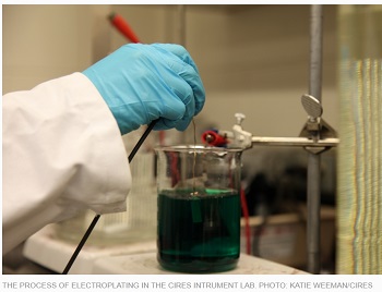
Electroplating, the process passing an electrical current through an aqueous solution of a dissolved metal to create a metal coating on a submerged object, is something David does almost daily. David’s work is in high demand in the research community: He and his team support science by plating instruments like charged-particle optics and components for cryogenics applications, and in this case, circuit boards for a team at NIST. They were looking for a metal plating that might be superconducting for the Pappas’s Quantum Processing Group at NIST. The team had unsuccessfully tried a number combinations, then one day David’s NIST colleague Xian Wu suggested they try rhenium: a hard, trace metal, with a high melting point, often used in the construction of jet engine turbines.
The team tested for electrical resistance, and were happy to see it superconduct up to 6K, well above the boiling temperature of liquid helium (4.2 K). The team is now investigating the role of hydrogen incorporation, interfaces, and strain on the enhanced superconducting temperature. But whatever the reason for the enhancement, being able to electroplate a superconductor is a giant step forward in the creation of tomorrow’s high-performance, superconducting computers.
Inside every computer there is a circuit board: a layered, electronic plank etched with thousands of conductive pathways. Pulses of electrical information called “bits” speed across the board, carrying out the computer’s functions. In regular computers, these electrical pulses are hindered by the material that comprises the board—electrical resistance slows down the electrons scurrying about the circuitry, and the wasted energy becomes heat. But with a superconductor, there is literally zero electrical resistance, so there is no heating. This efficiency will result in exceedingly fast and powerful computer systems.
Superconductors aren’t new, but the new paper presents evidence that electroplated rhenium may be the best material found to date for superconductive computer circuit board construction. Many other superconductive materials, like mercury or lead, are difficult to work with mechanically, have poor soldering properties, or melt at too-low temperatures. Even more impressively, the electroplating process would be easily scaled-up to mass-production, David said.
The team has applied for a provisional patent, and their work has already sparked interest from several technology giants and government sponsors.
Share on:


Suggested Items
The Chemical Connection: Reducing Etch System Water Usage, Part 2
05/02/2024 | Don Ball -- Column: The Chemical ConnectionIn my last column, I reviewed some relatively simple ways to reduce water usage in existing etch systems: cutting down cooling coil water flow, adding chillers to replace plant water for cooling, lowering flow rate nozzles for rinses, etc. This month, I’ll continue with more ways to control water usage in your etcher. Most of these are not easily retrofittable to existing equipment but should be given serious consideration when new equipment is contemplated. With the right combination of add-ons, it is possible to bring the amount of water used in an etch system to almost zero.
Designer’s Notebook: What Designers Need to Know About Manufacturing, Part 2
04/24/2024 | Vern Solberg -- Column: Designer's NotebookThe printed circuit board (PCB) is the primary base element for providing the interconnect platform for mounting and electrically joining electronic components. When assessing PCB design complexity, first consider the component area and board area ratio. If the surface area for the component interface is restricted, it may justify adopting multilayer or multilayer sequential buildup (SBU) PCB fabrication to enable a more efficient sub-surface circuit interconnect.
Insulectro’s 'Storekeepers' Extend Their Welcome to Technology Village at IPC APEX EXPO
04/03/2024 | InsulectroInsulectro, the largest distributor of materials for use in the manufacture of PCBs and printed electronics, welcomes attendees to its TECHNOLOGY VILLAGE during this year’s IPC APEX EXPO at the Anaheim Convention Center, April 9-11, 2024.
ENNOVI Introduces a New Flexible Circuit Production Process for Low Voltage Connectivity in EV Battery Cell Contacting Systems
04/03/2024 | PRNewswireENNOVI, a mobility electrification solutions partner, introduces a more advanced and sustainable way of producing flexible circuits for low voltage signals in electric vehicle (EV) battery cell contacting systems.
Heavy Copper PCBs: Bridging the Gap Between Design and Fabrication, Part 1
04/01/2024 | Yash Sutariya, Saturn Electronics ServicesThey call me Sparky. This is due to my talent for getting shocked by a variety of voltages and because I cannot seem to keep my hands out of power control cabinets. While I do not have the time to throw the knife switch to the off position, that doesn’t stop me from sticking screwdrivers into the fuse boxes. In all honesty, I’m lucky to be alive. Fortunately, I also have a talent for building high-voltage heavy copper circuit boards. Since this is where I spend most of my time, I can guide you through some potential design for manufacturability (DFM) hazards you may encounter with heavy copper design.