


 The Right Approach: I Hear the Train A Comin'
 It’s Only Common Sense: OCCAM—the Time Is Now
 Marcy's Musings: The Growing Industry
Flexible Fingerprint Sensors Promise Embedded Secure Access
May 18, 2018 | Holst CentreEstimated reading time: 2 minutes
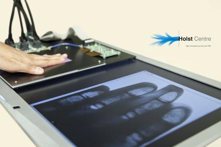
Researchers from Holst Centre have demonstrated a new class of flexible, large-area sensor technology for detecting finger- and palmprints. At less than 0.2 mm thick and with no bulky prisms or moving parts, the new sensors can be embedded into objects such as mobile phones and door handles to create "invisible" yet secure access control systems that can tell if the print is from a living person rather than a phantom or counterfeit.
The technology, which paves the way to low-cost sensors for large-area finger- and palmprint scanners, will be on show at the Innovation Zone at the Society for Information Display (SID) Display Week 2018 in Los Angeles, USA from 22 to 24 May, and the Imec Technology Forum (ITF) in Antwerp, Belgium from 23 to 24 May. Two demonstrators will showcase the technologies potential for high resolution and large active areas.
Measuring 6 x 8 cm, a 200-ppi demonstrator is large enough for 4-finger scanners that are currently used by border control authorities and delivers sufficient image quality for basic identification applications. Meanwhile, a slightly smaller 500-ppi demonstrator offer even higher image quality, compatible with FBI standards and enough for law enforcement agencies to visualize minutia and pores for more robust identification.
As with Holst Centre's earlier flexible X-ray detectors, the fingerprint sensors combine an organic photodiode frontplane, an oxide thin-film transistor (TFT) backplane (originally developed for flexible displays), and a thin-film barrier for protection against the environment. All three technological elements have been or are being transferred to industry for scale-up and commercialization.
The sensors read the finger- or palm print by detecting visible light (400 to 700 nm) reflected from the surface of the skin. However, they can also detect light that penetrates someway into the skin before being reflected. This allows them to sense a heartbeat from changes in the capillaries within the hand, and thus verify that the print comes from a live person.
Moreover, by using different photodiode materials, the sensors' capabilities can be extended to other wavelengths such as near infrared (NIR). This could enable new identification verification modes based on for example the pattern of veins in a hand, which is believed to be even more specific to an individual than a fingerprint. NIR sensors could also be used in other applications, such as blood oxygenation monitoring, or for night vision and 3D facial recognition.
"The flexible fingerprint sensor demonstrator shows the versatility and maturity of the flexible electronics technologies that Holst Centre is developing. With the underlying technology already in use in the flat-panel industry, there is a fast route to manufacturing and we are looking for industrial partners to take that step," says Hylke Akkerman, Program Manager at Holst Centre.
Share on:


Suggested Items
Koh Young Showcases Award-winning Inspection Solutions at SMTconnect with SmartRep in Hall 4A.225
04/25/2024 | Koh Young TechnologyKoh Young Technology, the industry leader in True 3D measurement-based inspection solutions, will showcase an array of award-winning inspection and measurement solutions at SMTconnect alongside its sales partner, SmartRep, in booth 4A.225 at NürnbergMesse from June 11-13, 2023. The following offers a glimpse into what Koh Young will present at the tradeshow:
Real Time with… IPC APEX EXPO 2024: Plasmatreat: Innovative Surface Preparation Solutions
04/25/2024 | Real Time with...IPC APEX EXPOIn this interview, Editor Nolan Johnson speaks with Hardev Grewal, CEO and president of Plasmatreat, a developer of atmospheric plasma solutions. Plasmatreat uses clean compressed air and electricity to create plasma, offering environmentally friendly methods for surface preparation. Their technology measures plasma density for process optimization and can remove organic micro-contamination. Nolan and Hardev also discuss REDOX-Tool, a new technology for removing metal oxides.
Nanotechnology Market to Surpass $53.51 Billion by 2031
04/25/2024 | PRNewswireSkyQuest projects that the nanotechnology market will attain a value of USD 53.51 billion by 2031, with a CAGR of 36.4% over the forecast period (2024-2031).
Cadence, TSMC Collaborate on Wide-Ranging Innovations to Transform System and Semiconductor Design
04/25/2024 | Cadence Design SystemsCadence Design Systems, Inc. and TSMC have extended their longstanding collaboration by announcing a broad range of innovative technology advancements to accelerate design, including developments ranging from 3D-IC and advanced process nodes to design IP and photonics.
SMC Korea 2024 to Highlight Semiconductor Materials Trends and Innovations on Industry’s Path to $1 Trillion
04/24/2024 | SEMIWith Korea a major consumer of semiconductor materials and advanced materials a key driver of innovation on the industry’s path to $1 trillion, industry leaders and experts will gather at SMC (Strategic Materials Conference) Korea 2024 on May 29 at the Suwon Convention Center in Gyeonggi-do, South Korea to provide insights into the latest materials developments and trends. Registration is open.