


 Marcy's Musings: The Growing Industry
 It’s Only Common Sense: Here’s What To Do After IPC APEX EXPO 2024
 Dan’s Biz Bookshelf: Seeing the How
Graphene Assembled Film Shows Higher Thermal Conductivity Than Graphite Film
June 21, 2018 | CHALMERS UNIVERSITY OF TECHNOLOGYEstimated reading time: 2 minutes
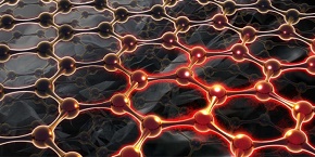
Researchers at Chalmers University of Technology, Sweden, have developed a graphene assembled film that has over 60% higher thermal conductivity than graphite film—despite the fact that graphite simply consists of many layers of graphene. The graphene film shows great potential as a novel heat spreading material for form-factor driven electronics and other high power-driven systems.
Until now, scientists in the graphene research community have assumed that graphene assembled film cannot have higher thermal conductivity than graphite film. Single layer graphene has a thermal conductivity between 3500 and 5000 W/mK. If you put two graphene layers together, then it theoretically becomes graphite, as graphene is only one layer of graphite.
Today, graphite films, which are practically useful for heat dissipation and spreading in mobile phones and other power devices, have a thermal conductivity of up to 1950 W/mK. Therefore, the graphene-assembled film should not have higher thermal conductivity than this.
Research scientists at Chalmers University of Technology have recently changed this situation. They discovered that the thermal conductivity of graphene assembled film can reach up to 3200 W/mK, which is over 60 percent higher than the best graphite films.
Professor Johan Liu and his research team have done this through careful control of both grain size and the stacking orders of graphene layers. The high thermal conductivity is a result of large grain size, high flatness, and weak interlayer binding energy of the graphene layers. With these important features, phonons, whose movement and vibration determine the thermal performance, can move faster in the graphene layers rather than interact between the layers, thereby leading to higher thermal conductivity.
“This is indeed a great scientific break-through, and it can have a large impact on the transformation of the existing graphite film manufacturing industry”, says Johan Liu.
Furthermore, the researchers discovered that the graphene film has almost three times higher mechanical tensile strength than graphite film, reaching 70 MPa.
“With the advantages of ultra-high thermal conductivity, and thin, flexible, and robust structures, the developed graphene film shows great potential as a novel heat spreading material for thermal management of form-factor driven electronics and other high power-driven systems”, says Johan Liu.
As a consequence of never-ending miniaturisation and integration, the performance and reliability of modern electronic devices and many other high-power systems are greatly threatened by severe thermal dissipation issues.
“To address the problem, heat spreading materials must get better properties when it comes to thermal conductivity, thickness, flexibility and robustness, to match the complex and highly integrated nature of power systems”, says Johan Liu. “Commercially available thermal conductivity materials, like copper, aluminum, and artificial graphite film, will no longer meet and satisfy these demands.”
The IP of the high-quality manufacturing process for the graphene film belongs to SHT Smart High Tech AB, a spin-off company from Chalmers, which is going to focus on the commercialisation of the technology.
Share on:


Suggested Items
Insulectro’s 'Storekeepers' Extend Their Welcome to Technology Village at IPC APEX EXPO
04/03/2024 | InsulectroInsulectro, the largest distributor of materials for use in the manufacture of PCBs and printed electronics, welcomes attendees to its TECHNOLOGY VILLAGE during this year’s IPC APEX EXPO at the Anaheim Convention Center, April 9-11, 2024.
ENNOVI Introduces a New Flexible Circuit Production Process for Low Voltage Connectivity in EV Battery Cell Contacting Systems
04/03/2024 | PRNewswireENNOVI, a mobility electrification solutions partner, introduces a more advanced and sustainable way of producing flexible circuits for low voltage signals in electric vehicle (EV) battery cell contacting systems.
Heavy Copper PCBs: Bridging the Gap Between Design and Fabrication, Part 1
04/01/2024 | Yash Sutariya, Saturn Electronics ServicesThey call me Sparky. This is due to my talent for getting shocked by a variety of voltages and because I cannot seem to keep my hands out of power control cabinets. While I do not have the time to throw the knife switch to the off position, that doesn’t stop me from sticking screwdrivers into the fuse boxes. In all honesty, I’m lucky to be alive. Fortunately, I also have a talent for building high-voltage heavy copper circuit boards. Since this is where I spend most of my time, I can guide you through some potential design for manufacturability (DFM) hazards you may encounter with heavy copper design.
Trouble in Your Tank: Supporting IC Substrates and Advanced Packaging, Part 5
03/19/2024 | Michael Carano -- Column: Trouble in Your TankDirect metallization systems based on conductive graphite or carbon dispersion are quickly gaining acceptance worldwide. Indeed, the environmental and productivity gains one can achieve with these processes are outstanding. In today’s highly competitive and litigious environment, direct metallization reduces costs associated with compliance, waste treatment, and legal issues related to chemical exposure. What makes these processes leaders in the direct metallization space?
AT&S Shines with Purest Copper on World Recycling Day
03/18/2024 | AT&SThe Styrian microelectronics specialist AT&S is taking World Recycling Day as an opportunity to review the progress that has been made in recent months at its sites around the world in terms of the efficient use of resources: