


 Marcy's Musings: The Growing Industry
 It’s Only Common Sense: Here’s What To Do After IPC APEX EXPO 2024
 Dan’s Biz Bookshelf: Seeing the How
Researchers Solve Major Challenge in Mass Production of Low-Cost Solar Cells
June 22, 2018 | New York University Tandon School of EngineeringEstimated reading time: 4 minutes
An international team of university researchers today reports solving a major fabrication challenge for perovskite cells — the intriguing potential challengers to silicon-based solar cells.
These crystalline structures show great promise because they can absorb almost all wavelengths of light. Perovskite solar cells are already commercialized on a small scale, but recent vast improvements in their power conversion efficiency (PCE) are driving interest in using them as low-cost alternatives for solar panels.
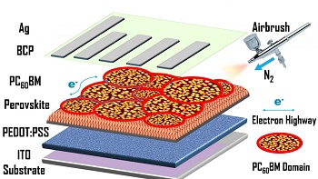
In the cover article published online today for the June 28, 2018 issue of Nanoscale, a publication of the Royal Society of Chemistry, the research team reveals a new scalable means of applying a critical component to perovskite cells to solve some major fabrication challenges. The researchers were able to apply the critical electron transport layer (ETL) in perovskite photovoltaic cells in a new way — spray coating — to imbue the ETL with superior conductivity and a strong interface with its neighbor, the perovskite layer.
The research is led by André D. Taylor, an associate professor in the NYU Tandon School of Engineering’s Chemical and Biomolecular Engineering Department, with Yifan Zheng, the first author on the paper and a Peking University researcher. Co-authors are from the University of Electronic Science and Technology of China, Yale University, and Johns Hopkins University.
Most solar cells are “sandwiches” of materials layered in such a way that when light hits the cell’s surface, it excites electrons in negatively charged material and sets up an electric current by moving the electrons toward a latticework of positively charged “holes.” In perovskite solar cells with a simple planar orientation called p-i-n (or n-i-p when inverted), the perovskite constitutes the light-trapping intrinsic layer (the “i” in p-i-n) between the negatively charged ETL and a positively charged hole transport layer (HTL).
When the positively and negatively charged layers are separated, the architecture behaves like a subatomic game of Pachinko in which photons from a light source dislodge unstable electrons from the ETL, causing them to fall toward the positive HTL side of the sandwich. The perovskite layer expedites this flow. While perovskite makes for an ideal intrinsic layer because of its strong affinity both for holes and electrons and its quick reaction time, commercial-scale fabrication has proved challenging partly because it is difficult to effectively apply a uniform ETL layer over the crystalline surface of the perovskite.
The researchers chose the compound [6,6]-phenyl-C(61)-butyric acid methyl ester (PCBM) because of its track record as an ETL material and because PCBM applied in a rough layer offers the possibility of improved conductivity, less-penetrable interface contact, and enhanced light trapping.
“Very little research has been done on ETL options for the planar p-i-n design,” said Taylor. “The key challenge in planar cells is, how do you actually assemble them in a way that doesn’t destroy the adjacent layers?”
The most common method is spin casting, which involves spinning the cell and allowing centripetal force to disperse the ETL fluid over the perovskite substrate. But this technique is limited to small surfaces and results in an inconsistent layer that lowers the performance of the solar cell. Spin casting is also inimicable to commercial production of large solar panels by such methods as roll-to-roll manufacture, for which the flexible p-i-n planar perovskite architecture is otherwise well suited.
The researchers instead turned to spray coating, which applies the ETL uniformly across a large area and is suitable for manufacturing large solar panels. They reported a 30 percent efficiency gain over other ETLs – from a PCE of 13 percent to over 17 percent – and fewer defects.
Added Taylor, “Our approach is concise, highly reproducible, and scalable. It suggests that spray coating the PCBM ETL could have broad appeal toward improving the efficiency baseline of perovskite solar cells and providing an ideal platform for record-breaking p-i-n perovskite solar cells in the near future.”
The Foundation of the National Natural Science Foundation of China (NSFC), the Foundation for Innovation Research Groups of the NSFC, the Chinese Scholarship Council, and the U.S. National Science Foundation provided funding for the study.
About the New York University Tandon School of Engineering
The NYU Tandon School of Engineering dates to 1854, the founding date for both the New York University School of Civil Engineering and Architecture and the Brooklyn Collegiate and Polytechnic Institute (widely known as Brooklyn Poly). A January 2014 merger created a comprehensive school of education and research in engineering and applied sciences, rooted in a tradition of invention and entrepreneurship and dedicated to furthering technology in service to society. In addition to its main location in Brooklyn, NYU Tandon collaborates with other schools within NYU, one of the country’s foremost private research universities, and is closely connected to engineering programs at NYU Abu Dhabi and NYU Shanghai. It operates Future Labs focused on start-up businesses in downtown Manhattan and Brooklyn and an award-winning online graduate program. For more information, visit engineering.nyu.edu.
Share on:


Suggested Items
Ansys Joins BAE Systems’ Mission Advantage Program to Advance Digital Engineering Across US Department of Defense
04/16/2024 | ANSYSAnsys announced it is working with BAE Systems, Inc., to accelerate the adoption of digital engineering and MBSE across the Department of Defense (DoD).
Incap Estonia Teamed Up With Solaride to Fuel Youth Excitement for The World of Engineering
04/11/2024 | IncapIncap Estonia partnered with Solaride to ignite enthusiasm among young people for the world of engineering and sustainable technology. Together, they organised an inspiring day for students from grades 7 through 12 in Saaremaa. Held at Incap’s Kuressaare factory, this event brought together over 130 young minds eager to explore the innovative world of technology and learn more about advanced electronics manufacturing.
Mark Schulman Rocks Zuken Innovation World + integrate24
04/10/2024 | ZukenZuken USA, Inc. is excited to announce that the renowned drummer and motivational speaker, Mark Schulman, will be the keynote speaker at this year's Zuken Innovation World Americas (ZIW) conference, co-located with integrate24. Scheduled for September 17-19, 2024, in the vibrant city of Cleveland, Ohio, the conference aims to bring together the brightest minds in the PCB, Wire Harness, and Digital Engineering fields.
Saab Announces Plans for New Munitions Facility in U.S.
04/03/2024 | SaabSaab announced plans to build a new munitions facility in the U.S., continuing the company’s strong investment and growth domestically.
NextFlex Announces 2024 Fellows Awards for Five Outstanding Recipients
03/29/2024 | BUSINESS WIRENextFlex, America's Hybrid Electronics Manufacturing Institute, presented the annual NextFlex Fellow Awards to five deserving individuals in recognition of their exceptional commitment to advanced manufacturing and the additive hybrid electronics member community.