


 It’s Only Common Sense: OCCAM—the Time Is Now
 Marcy's Musings: The Growing Industry
 Dan’s Biz Bookshelf: Seeing the How
No Barrier to Applications for a Remarkable 2D Material
June 25, 2018 | A*STAREstimated reading time: 1 minute
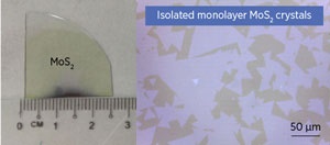
Mass production of large, uniform sheets of single-layer molybdenum disulfide, MoS2, is difficult, which limits its commercial application. A*STAR researchers have modified an existing manufacturing technique to enable the use of MoS2 in a range of technologies from photodevices to flexible, transparent sensors.
The two-dimensional material has attracted considerable attention because of its extraordinary physical, electronic and optoelectronic properties, including flexibility, transparency and semiconducting characteristics. But fabricating large-scale, defect-free single layers of MoS2 is highly challenging.
Dongzhi Chi and his team from the A*STAR Institute of Materials Research and Engineering, in collaboration with colleagues from the National University of Singapore and the Indian Institute of Science Education and Research, has modified a current technique, known as chemical vapor deposition (CVD), so that it can now produce uniform, centimeter-sized sheets of MoS2 crystals with large grain sizes.
“The physical properties of MoS2 vary greatly with its thickness,” explains Chi, “to maintain its remarkable electronic and physical properties we need a method that can uniformly deposit MoS2 films over a large area with high crystallinity.”
Although CVD is an effective technique for fabricating large-area, uniform sheets of MoS2 of varying thickness on different substrates, and significant progress has been made in improving the quality of MoS2 monolayers produced by the technique, little attention has been paid to controlling the chemical vapors using physical barriers during the growth of MoS2 crystals.
By introducing a nickel oxide (NiO) barrier, the researchers were able to control the concentration and distribution of chemical vapors during the growth of MoS2 crystals. Because NiO reacts with molybdenum trioxide (MoO3), one of the chemical reactants used in the growth process, it traps and lowers the MoO3 concentration, allowing the uniform deposition of monolayers of MoS2 over a large area.
“The advantage of this approach is the ease of implementation as well as a reduction in contamination, and it allows for control of the chemical exposure during the growth process,” says Chi.
The work has led to further advances in the fabrication of uniform and large-area MoS2 monolayers, and could also be applied to other two-dimensional materials.
“We are now looking to scale up our fabrication process for producing even larger sheets, which could pave the way for next-generation optoelectronic and sensor technologies,” says Chi.
Share on:


Suggested Items
Koh Young Showcases Award-winning Inspection Solutions at SMTconnect with SmartRep in Hall 4A.225
04/25/2024 | Koh Young TechnologyKoh Young Technology, the industry leader in True 3D measurement-based inspection solutions, will showcase an array of award-winning inspection and measurement solutions at SMTconnect alongside its sales partner, SmartRep, in booth 4A.225 at NürnbergMesse from June 11-13, 2023. The following offers a glimpse into what Koh Young will present at the tradeshow:
Real Time with… IPC APEX EXPO 2024: Plasmatreat: Innovative Surface Preparation Solutions
04/25/2024 | Real Time with...IPC APEX EXPOIn this interview, Editor Nolan Johnson speaks with Hardev Grewal, CEO and president of Plasmatreat, a developer of atmospheric plasma solutions. Plasmatreat uses clean compressed air and electricity to create plasma, offering environmentally friendly methods for surface preparation. Their technology measures plasma density for process optimization and can remove organic micro-contamination. Nolan and Hardev also discuss REDOX-Tool, a new technology for removing metal oxides.
KYZEN to Promote Pair of Stencil Cleaning Chemistries at SMTA Ciudad Jaurez Expo & Tech Forum
04/25/2024 | KYZEN'KYZEN, the global leader in innovative environmentally friendly cleaning chemistries, will exhibit at the SMTA Ciudad Juarez Expo & Tech Forum, scheduled to take place Thursday, May 9, 2024 at the Injectronic Convention Center in Ciudad Jaurez, Chihuahua, Mexico. During the event the KYZEN Clean Team will focus on understencil cleaning products KYZEN E5631J and CYBERSOLV C8882.
Cadence, TSMC Collaborate on Wide-Ranging Innovations to Transform System and Semiconductor Design
04/25/2024 | Cadence Design SystemsCadence Design Systems, Inc. and TSMC have extended their longstanding collaboration by announcing a broad range of innovative technology advancements to accelerate design, including developments ranging from 3D-IC and advanced process nodes to design IP and photonics.
Listen Up! The Intricacies of PCB Drilling Detailed in New Podcast Episode
04/25/2024 | I-Connect007In episode 5 of the podcast series, On the Line With: Designing for Reality, Nolan Johnson and Matt Stevenson continue down the manufacturing process, this time focusing on the post-lamination drilling process for PCBs. Matt and Nolan delve into the intricacies of the PCB drilling process, highlighting the importance of hole quality, drill parameters, and design optimization to ensure smooth manufacturing. The conversation covers topics such as drill bit sizes, aspect ratios, vias, challenges in drilling, and ways to enhance efficiency in the drilling department.