


 It’s Only Common Sense: OCCAM—the Time Is Now
 Marcy's Musings: The Growing Industry
 Dan’s Biz Bookshelf: Seeing the How
Closing the Gap: On the Road to Terahertz Electronics
June 26, 2018 | TUMEstimated reading time: 2 minutes
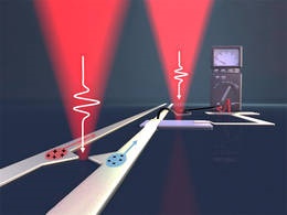
A team headed by the TUM physicists Alexander Holleitner and Reinhard Kienberger has succeeded for the first time in generating ultrashort electric pulses on a chip using metal antennas only a few nanometers in size, then running the signals a few millimeters above the surface and reading them in again a controlled manner. The technology enables the development of new, powerful terahertz components.
Image caption: Pulses of femtosecond length from the pump laser (left) generate on-chip electric pulses in the terahertz frequency range. With the right laser, the information is read out again. (Image: Christoph Hohmann / NIM, Holleitner / TUM)
Classical electronics allows frequencies up to around 100 gigahertz. Optoelectronics uses electromagnetic phenomena starting at 10 terahertz. This range in between is referred to as the terahertz gap, since components for signal generation, conversion and detection have been extremely difficult to implement.
The TUM physicists Alexander Holleitner and Reinhard Kienberger succeeded in generating electric pulses in the frequency range up to 10 terahertz using tiny, so-called plasmonic antennas and run them over a chip. Researchers call antennas plasmonic if, because of their shape, they amplify the light intensity at the metal surfaces.
Asymmetric antennas
The shape of the antennas is important. They are asymmetrical: One side of the nanometer-sized metal structures is more pointed than the other. When a lens-focused laser pulse excites the antennas, they emit more electrons on their pointed side than on the opposite flat ones. An electric current flows between the contacts – but only as long as the antennas are excited with the laser light.
"In photoemission, the light pulse causes electrons to be emitted from the metal into the vacuum," explains Christoph Karnetzky, lead author of the Nature work. "All the lighting effects are stronger on the sharp side, including the photoemission that we use to generate a small amount of current."
Ultrashort terahertz signals
The light pulses lasted only a few femtoseconds. Correspondingly short were the electrical pulses in the antennas. Technically, the structure is particularly interesting because the nano-antennas can be integrated into terahertz circuits a mere several millimeters across.
In this way, a femtosecond laser pulse with a frequency of 200 terahertz could generate an ultra-short terahertz signal with a frequency of up to 10 terahertz in the circuits on the chip, according to Karnetzky.
The researchers used sapphire as the chip material because it cannot be stimulated optically and, thus, causes no interference. With an eye on future applications, they used 1.5-micron wavelength lasers deployed in traditional internet fiber-optic cables.
An amazing discovery
Holleitner and his colleagues made yet another amazing discovery: Both the electrical and the terahertz pulses were non-linearly dependent on the excitation power of the laser used. This indicates that the photoemission in the antennas is triggered by the absorption of multiple photons per light pulse.
"Such fast, nonlinear on-chip pulses did not exist hitherto," says Alexander Holleitner. Utilizing this effect he hopes to discover even faster tunnel emission effects in the antennas and to use them for chip applications.
Share on:


Suggested Items
Water Management in a Large Printed Circuit Board Manufacturer
04/15/2024 | Charles Nehrig, TTM TechnologiesTTM’s environmental management is grounded in its Environmental Statement and Environmental Policy, which promote measures that make for a more responsible environmental management process. Our management system helps TTM work toward minimizing its environmental footprint and increasing the sustainability of its operations. TTM monitors its environmental performance just as it monitors its operational performance, and provides the resources required to adhere to the Company’s environmental responsibilities.
Happy’s Tech Talk #27: Integrated Mesh Power System (IMPS) for PCBs
04/08/2024 | Happy Holden -- Column: Happy’s Tech TalkA significant decrease in HDI substrate production cost can be achieved by reducing the number of substrate layers from conventional through-hole multilayers and microvia multilayers of eight, 10, 12, and more to only two layers. Besides reducing direct processing steps, the yield will increase as defect-producing operations are eliminated. The integrated mesh power system (IMPS) was invented in the latter years of MCM-D use for thin-film fabrication. Those geometries fit today into our use of ultra HDI.
Trouble in Your Tank: Supporting IC Substrates and Advanced Packaging, Part 5
03/19/2024 | Michael Carano -- Column: Trouble in Your TankDirect metallization systems based on conductive graphite or carbon dispersion are quickly gaining acceptance worldwide. Indeed, the environmental and productivity gains one can achieve with these processes are outstanding. In today’s highly competitive and litigious environment, direct metallization reduces costs associated with compliance, waste treatment, and legal issues related to chemical exposure. What makes these processes leaders in the direct metallization space?
Indium Corporation Experts to Present at SEMI THERM
03/07/2024 | Indium CorporationIndium Corporation Global Account Manager and Senior Thermal Technologist Tim Jensen and Product Development Specialist for Thermal Interface Materials Miloš Lazić will present on thermal interface material (TIM) technology at SEMI-THERM, taking place March 25–28 in San Jose, California, U.S.
Indium Corporation to Showcase Proven EV Products and High-Reliability Alloys at Productronica China
02/28/2024 | Indium CorporationAs a materials pioneer and trusted partner in electric vehicle (EV) and e-Mobility manufacturing, Indium Corporation is proud to showcase its high-reliability alloys and soldering solutions at Productronica China, March 20-22, in Shanghai.