


 The Right Approach: I Hear the Train A Comin'
 It’s Only Common Sense: OCCAM—the Time Is Now
 Marcy's Musings: The Growing Industry
New Insights Bolster Einstein’s Idea about How Heat Moves Through Solids
June 29, 2018 | ORNLEstimated reading time: 3 minutes
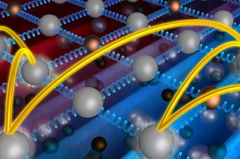
A discovery by scientists at the Department of Energy’s Oak Ridge National Laboratory supports a century-old theory by Albert Einstein that explains how heat moves through everything from travel mugs to engine parts.
The transfer of heat is fundamental to all materials. This new research, published in the journal Science, explored thermal insulators, which are materials that block transmission of heat.
“We saw evidence for what Einstein first proposed in 1911—that heat energy hops randomly from atom to atom in thermal insulators,” said Lucas Lindsay, materials theorist at ORNL. “The hopping is in addition to the normal heat flow through the collective vibration of atoms.”
The random energy hopping is not noticeable in materials that conduct heat well, like copper on the bottom of saucepans during cooking, but may be detectable in solids that are less able to transmit heat.
This observation advances understanding of heat conduction in thermal insulators and will aid the discovery of novel materials for applications from thermoelectrics that recover waste heat to barrier coatings that prevent transmission of heat.
Lindsay and his colleagues used sophisticated vibration-sensing tools to detect the motion of atoms and supercomputers to simulate the journey of heat through a simple thallium-based crystal. Their analysis revealed that the atomic vibrations in the crystal lattice were too sluggish to transmit much heat.
“Our predictions were two times lower than we observed from our experiments. We were initially baffled,” Lindsay said. “This led to the observation that another heat transfer mechanism must be at play.”
Knowing that the second heat transfer channel of random energy hopping exists will inform researchers on how to choose materials for heat management applications. This finding, if applied, could drastically reduce energy costs, carbon emissions and waste heat.
Many useful materials, such as silicon, have a chemically bonded latticework of atoms. Heat is usually carried through this lattice by atomic vibrations, or sound waves. These heat-bearing waves bump into each other, which slows the transfer of heat.
“The thallium-based material we studied has one of the lowest thermal conductivities of any crystal,” Lindsay said. “Much of the vibrating energy is confined to single atoms, and the energy then hops randomly through the crystal.”
“Both the sound waves and the heat-hopping mechanism first theorized by Einstein characterize a two-channel model, and not only in this material, but in several other materials that also demonstrate ultralow conductivity,” said ORNL materials scientist David Parker.
For now, heat-hopping may only be detectable in excellent thermal insulators. “However, this heat-hopping channel may well be present in other crystalline solids, creating a new lever for managing heat,” he said.
The study’s lead coauthor was Saikat Mukhopadhyay, a former postdoctoral research associate at ORNL and currently a National Research Council research associate at the U.S. Naval Research Laboratory.
Additional coauthors of the paper titled, “Two-channel model for ultralow thermal conductivity of crystalline Tl3VSe4,” included ORNL’s David S. Parker, Brian C. Sales, Alexander A. Puretzky, Michael A. McGuire and Lucas Lindsay.
This work was supported by the Department of Energy’s Office of Science. Raman spectroscopy measurements were made at the Center for Nanophase Materials Sciences, and the study used computational resources from the National Energy Research Scientific Computing Center at DOE’s Lawrence Berkeley National Laboratory. Both centers are DOE Office of Science User Facilities.
ORNL is managed by UT-Battelle for DOE’s Office of Science. The Office of Science is the single largest supporter of basic research in the physical sciences in the United States, and is working to address some of the most pressing challenges of our time. For more information, please click here.
Share on:


Suggested Items
Designer’s Notebook: What Designers Need to Know About Manufacturing, Part 2
04/24/2024 | Vern Solberg -- Column: Designer's NotebookThe printed circuit board (PCB) is the primary base element for providing the interconnect platform for mounting and electrically joining electronic components. When assessing PCB design complexity, first consider the component area and board area ratio. If the surface area for the component interface is restricted, it may justify adopting multilayer or multilayer sequential buildup (SBU) PCB fabrication to enable a more efficient sub-surface circuit interconnect.
Insulectro’s 'Storekeepers' Extend Their Welcome to Technology Village at IPC APEX EXPO
04/03/2024 | InsulectroInsulectro, the largest distributor of materials for use in the manufacture of PCBs and printed electronics, welcomes attendees to its TECHNOLOGY VILLAGE during this year’s IPC APEX EXPO at the Anaheim Convention Center, April 9-11, 2024.
ENNOVI Introduces a New Flexible Circuit Production Process for Low Voltage Connectivity in EV Battery Cell Contacting Systems
04/03/2024 | PRNewswireENNOVI, a mobility electrification solutions partner, introduces a more advanced and sustainable way of producing flexible circuits for low voltage signals in electric vehicle (EV) battery cell contacting systems.
Heavy Copper PCBs: Bridging the Gap Between Design and Fabrication, Part 1
04/01/2024 | Yash Sutariya, Saturn Electronics ServicesThey call me Sparky. This is due to my talent for getting shocked by a variety of voltages and because I cannot seem to keep my hands out of power control cabinets. While I do not have the time to throw the knife switch to the off position, that doesn’t stop me from sticking screwdrivers into the fuse boxes. In all honesty, I’m lucky to be alive. Fortunately, I also have a talent for building high-voltage heavy copper circuit boards. Since this is where I spend most of my time, I can guide you through some potential design for manufacturability (DFM) hazards you may encounter with heavy copper design.
Trouble in Your Tank: Supporting IC Substrates and Advanced Packaging, Part 5
03/19/2024 | Michael Carano -- Column: Trouble in Your TankDirect metallization systems based on conductive graphite or carbon dispersion are quickly gaining acceptance worldwide. Indeed, the environmental and productivity gains one can achieve with these processes are outstanding. In today’s highly competitive and litigious environment, direct metallization reduces costs associated with compliance, waste treatment, and legal issues related to chemical exposure. What makes these processes leaders in the direct metallization space?