


 It’s Only Common Sense: OCCAM—the Time Is Now
 Marcy's Musings: The Growing Industry
 Dan’s Biz Bookshelf: Seeing the How
Ultimate Precision for Sensor Technology Using Qubits and Machine Learning
July 3, 2018 | Aalto UniversityEstimated reading time: 3 minutes
Extracting information quickly from quantum states is necessary for future quantum processors and super-sensitive detectors in existing technologies.
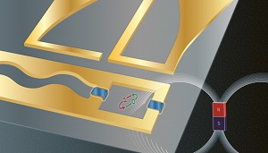
Image caption: An artificial atom realized from superconducting strips of aluminum on a silicon chip can be employed for the detection of magnetic fields. Image: Babi Brasileiro / Aalto University
There are limits to how accurately you can measure things. Think of an X-ray image: it is likely quite blurry and something only an expert physician can interpret properly. The contrast between different tissues is rather poor but could be improved by longer exposure times, higher intensity, or by taking several images and overlapping them. But there are considerable limitations: humans can safely be exposed to only so much radiation, and imaging takes time and resources.
A well-established rule of thumb is the so-called standard quantum limit: the precision of the measurement scales inversely with the square root of available resources. In other words, the more resources—time, radiation power, number of images, etc.—you throw in, the more accurate your measurement will be. This will, however, only get you so far: extreme precision also means using excessive resources.
A team of researchers from Aalto University, ETH Zurich, and MIPT and Landau Institute in Moscow have pushed the envelope and came up with a way to measure magnetic fields using a quantum system. They demonstrate a new method that combines quantum phenomena and machine learning to realise a magnetometer with accuracy beyond the standard quantum limit.
The detection of magnetic fields is important in a variety of fields, from geological prospecting to imaging brain activity. The researchers believe that their work is a first step towards of using quantum-enhanced methods for sensor technology.
“We wanted to design a highly efficient but minimally invasive measurement technique. Imagine, for example, extremely sensitive samples: we have to either use as low intensities as possible to observe the samples or push the measurement time to a minimum,” explains Sorin Paraoanu, leader of the Kvantti research group at Aalto University.
Their paper, published in the prestigious journal npj Quantum Information shows how to improve the accuracy of magnetic field measurements by exploiting the coherence of a superconducting artificial atom, a qubit. It is a tiny device made of overlapping strips of aluminium evaporated on a silicon chip—a technology similar to the one used to fabricate the processors of mobile phones and computers.
When the device is cooled to a very low temperature, magic happens: the electrical current flows in it without any resistance and starts to display quantum mechanical properties similar to those of real atoms. When irradiated with a microwave pulse—not unlike the ones in household microwave ovens—the state of the artificial atom changes. It turns out that this change depends on the external magnetic field applied: measure the atom and you will figure out the magnetic field.
But to surpass the standard quantum limit, yet another trick had to be performed using a technique similar to a widely-applied branch of machine learning, pattern recognition.
“We use an adaptive technique: first, we perform a measurement, and then, depending on the result, we let our pattern recognition algorithm decide how to change a control parameter in the next step in order to achieve the fastest estimation of the magnetic field,” explains Andrey Lebedev, corresponding author from ETH Zurich, now at MIPT in Moscow.
“This is a nice example of quantum technology at work: by combining a quantum phenomenon with a measurement technique based on supervised machine learning, we can enhance the sensitivity of magnetic field detectors to a realm that clearly breaks the standard quantum limit,” Lebedev says.
Share on:


Suggested Items
Inkjet Solder Mask ‘Has Arrived’
04/10/2024 | Pete Starkey, I-Connect007I was delighted to be invited to attend an interactive webinar entitled “Solder Mask Coating Made Easy with Additive Manufacturing,” hosted by SUSS MicroTec Netherlands in Eindhoven. The webinar was introduced and moderated by André Bodegom, managing director at Adeon Technologies, and the speakers were Mariana Van Dam, senior product manager PCB imaging solutions at AGFA in Belgium; Ashley Steers, sales manager at Electra Polymers in the UK; and Dr. Luca Gautero, product manager at SUSS MicroTec Netherlands.
NetVia Group Acquires Direct Imaging from Mivatek
04/09/2024 | Miva TechnologiesMiva Technologies is pleased to announce NetVia Group, Irving, TX has acquired a new Miva 2400NG Dual Tray Direct Imaging System with 30-micron capabilities for inner, outer and soldermask imaging.
Teledyne to Acquire Adimec
02/13/2024 | TeledyneTeledyne Technologies Incorporated announced that it has entered into an agreement to acquire Adimec Holding B.V. and its subsidiaries.
Real Time with... productronica 2023: MivaTek Global Advances Technology With High-res Imaging System
12/08/2023 | Real Time with...productronicaMivaTek's Brendan Hogan talks about how the company employs Digitally Adaptive Rasterization Technology (DART) in their high-res imaging equipment. He also shares how the blurred line between semiconductors and microelectronics is driving broader application of the imaging process.
Keysight Enables Validation of Arbe 4D Imaging Radar Chipset
11/30/2023 | Keysight Technologies, Inc.Keysight Technologies, Inc. announces that Arbe has selected the E8719A Radar Target Solution (RTS) to test the Arbe 4D imaging radar chipset for automotive applications.