


 The Right Approach: I Hear the Train A Comin'
 It’s Only Common Sense: OCCAM—the Time Is Now
 Marcy's Musings: The Growing Industry
Using Spin Current to Convert Mechanical Vibrations Into Electricity
July 20, 2018 | RIKENEstimated reading time: 2 minutes
A nanoscale device that converts mechanical ripples into an electrical current via a ‘spin current’ has been made by RIKEN researchers1. Further development of this technology could see it used in devices that permit sound waves to pass in one direction but block them in the opposite direction.
Conventional electronic devices are based on shunting electrons around circuits. Because electrons possess charge, they give rise to electric currents when they move. The emerging field of spintronics, however, harnesses another property of electrons: their spin. Spin currents are the spintronic equivalent of electric currents, but unlike electric currents, they can flow without the electrons actually moving since spin can be transferred between stationary electrons.
As well as holding out the promise of resistance-free energy flow, electron spin can be used to convert between various forms of energy, including electricity, light, sound, vibrations and heat. This ability to switch between different energy forms will lead to a wide range of versatile devices.
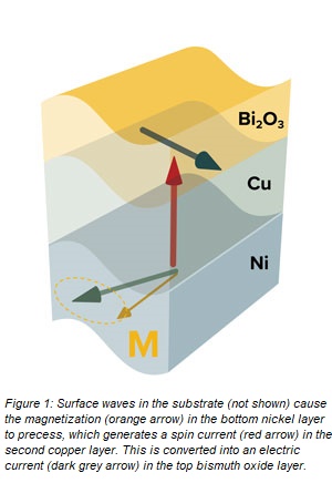
Jorge Puebla at the RIKEN Center for Emergent Matter Science and Mingran Xu at the University of Tokyo and colleagues have made a three-layered nanodevice that converts mechanical vibrations into electric current. Waves generated on the surface of a substrate cause the magnetization of the bottom nickel layer of the device to sweep out arcs (Fig. 1). This periodic motion of the magnetization generates a spin current in the second copper layer. Finally, the spin current is converted into an electric current at the interface with the top bismuth oxide layer.
The team found that the spin current generated in the second layer was particularly large. “In our field, researchers are seeking to generate higher spin currents,” explains Xu. “Our method produces quite a huge spin current.”
“We’re approaching spin currents that are large enough to move magnetic domain walls, which could be used in memory devices,” adds Puebla. “We’re still below the spin currents needed, but believe we should be able to get close by optimizing our devices.”
Another advance was the use of a relatively new way to convert a spin current into an electrical one. Often expensive metals such as platinum are required for this conversion, but the method the team used worked with copper. “I think in terms of technology, people might find this approach cheaper to produce real devices,” comments Xu.
Since the output varied with direction, a potential application is audio devices that allow sound to flow in one direction but not the opposite one. “You could have headphones that allow you to listen to music and hear what others are saying, but other people cannot hear what you’re listening to,” says Puebla.
Share on:


Suggested Items
Designer’s Notebook: What Designers Need to Know About Manufacturing, Part 2
04/24/2024 | Vern Solberg -- Column: Designer's NotebookThe printed circuit board (PCB) is the primary base element for providing the interconnect platform for mounting and electrically joining electronic components. When assessing PCB design complexity, first consider the component area and board area ratio. If the surface area for the component interface is restricted, it may justify adopting multilayer or multilayer sequential buildup (SBU) PCB fabrication to enable a more efficient sub-surface circuit interconnect.
Insulectro’s 'Storekeepers' Extend Their Welcome to Technology Village at IPC APEX EXPO
04/03/2024 | InsulectroInsulectro, the largest distributor of materials for use in the manufacture of PCBs and printed electronics, welcomes attendees to its TECHNOLOGY VILLAGE during this year’s IPC APEX EXPO at the Anaheim Convention Center, April 9-11, 2024.
ENNOVI Introduces a New Flexible Circuit Production Process for Low Voltage Connectivity in EV Battery Cell Contacting Systems
04/03/2024 | PRNewswireENNOVI, a mobility electrification solutions partner, introduces a more advanced and sustainable way of producing flexible circuits for low voltage signals in electric vehicle (EV) battery cell contacting systems.
Heavy Copper PCBs: Bridging the Gap Between Design and Fabrication, Part 1
04/01/2024 | Yash Sutariya, Saturn Electronics ServicesThey call me Sparky. This is due to my talent for getting shocked by a variety of voltages and because I cannot seem to keep my hands out of power control cabinets. While I do not have the time to throw the knife switch to the off position, that doesn’t stop me from sticking screwdrivers into the fuse boxes. In all honesty, I’m lucky to be alive. Fortunately, I also have a talent for building high-voltage heavy copper circuit boards. Since this is where I spend most of my time, I can guide you through some potential design for manufacturability (DFM) hazards you may encounter with heavy copper design.
Trouble in Your Tank: Supporting IC Substrates and Advanced Packaging, Part 5
03/19/2024 | Michael Carano -- Column: Trouble in Your TankDirect metallization systems based on conductive graphite or carbon dispersion are quickly gaining acceptance worldwide. Indeed, the environmental and productivity gains one can achieve with these processes are outstanding. In today’s highly competitive and litigious environment, direct metallization reduces costs associated with compliance, waste treatment, and legal issues related to chemical exposure. What makes these processes leaders in the direct metallization space?