


 Marcy's Musings: The Growing Industry
 It’s Only Common Sense: Here’s What To Do After IPC APEX EXPO 2024
 Dan’s Biz Bookshelf: Seeing the How
Printing Solar Cells and Organic LEDs
August 23, 2018 | HZBEstimated reading time: 2 minutes
Humboldt-Universität zu Berlin and Helmholtz-Zentrum Berlin form a joint lab and research group “Generative production processes for hybrid components”.
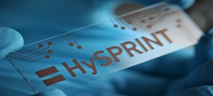
Image Caption: The HySPRINT logo (Helmholtz Innovation Lab) printed on a copper solution symbolizes how the thinnest material layers can be produced simply and cost-effectively. Possible applications are solar cells, organic LEDs or transistors. Photo credit: Humboldt Universität zu Berlin/List-Kratochvil
Solar cells, LEDs and detectors made of organic and hybrid semiconductors can nowadays be simply printed out, even together with teensy nanostructures that make them function better. The development of low-cost printing methods for electronic and optoelectronic components is at the centre of things for the new joint research group and the joint laboratory of the Helmholtz-Zentrum Berlin (HZB) and Humboldt-Universität zu Berlin (HU).
Cooperating together in the new research group are the HU workgroup “Hybrid Devices” led by Prof. Dr. Emil List-Kratochvil, the HZB young investigator group of Dr. Eva Unger, the Helmholtz Innovation Lab HySPRINT, and the Competence Centre Photovoltaics Berlin (PVcomB) directed by Prof. Dr. Rutger Schlatmann. The partners are building up a joint lab at Humboldt-Universität zu Berlin that will allow the researchers to acquire and use complementary laboratory infrastructures for various coating methods.
Prof. Emil List-Kratochvil is the head of the HU workgroup “Hybrid Devices” at IRIS Adlershof, and has been working for 15 years on developing electronic and optoelectronic hybrid components, resource-efficient deposition techniques (inkjet printing) and in-situ nanostructuring and synthetic methods. This expertise complements the aims of the HZB young investigator group led by Dr. Eva Unger. She will be developing solution-based manufacturing methods for depositing perovskite semiconductor layers onto larger surface areas for solar cells. “The new research group with List-Kratochvil is a real win for us. With his experience in printed electronic components, he is an ideal cooperation partner for us,” Unger says.
In recent months, the researcher and her team have already come much closer to her goal of developing hybrid tandem solar cells with large-surface-areas in the scope of the Helmholtz Innovation Lab HySPRINT. Now, the next step is to upscale the process in order to drive the novel solar cells towards market maturity. The Competence Centre Thin-Film- and Nanotechnology for Photovoltaics Berlin (PVcomB) is the ideal partner for the development of industrially relevant manufacturing processes. The joint research group is now striving towards building a pilot line on which to develop prototypes of hybrid components.
Share on:


Suggested Items
Insulectro’s 'Storekeepers' Extend Their Welcome to Technology Village at IPC APEX EXPO
04/03/2024 | InsulectroInsulectro, the largest distributor of materials for use in the manufacture of PCBs and printed electronics, welcomes attendees to its TECHNOLOGY VILLAGE during this year’s IPC APEX EXPO at the Anaheim Convention Center, April 9-11, 2024.
ENNOVI Introduces a New Flexible Circuit Production Process for Low Voltage Connectivity in EV Battery Cell Contacting Systems
04/03/2024 | PRNewswireENNOVI, a mobility electrification solutions partner, introduces a more advanced and sustainable way of producing flexible circuits for low voltage signals in electric vehicle (EV) battery cell contacting systems.
Heavy Copper PCBs: Bridging the Gap Between Design and Fabrication, Part 1
04/01/2024 | Yash Sutariya, Saturn Electronics ServicesThey call me Sparky. This is due to my talent for getting shocked by a variety of voltages and because I cannot seem to keep my hands out of power control cabinets. While I do not have the time to throw the knife switch to the off position, that doesn’t stop me from sticking screwdrivers into the fuse boxes. In all honesty, I’m lucky to be alive. Fortunately, I also have a talent for building high-voltage heavy copper circuit boards. Since this is where I spend most of my time, I can guide you through some potential design for manufacturability (DFM) hazards you may encounter with heavy copper design.
Trouble in Your Tank: Supporting IC Substrates and Advanced Packaging, Part 5
03/19/2024 | Michael Carano -- Column: Trouble in Your TankDirect metallization systems based on conductive graphite or carbon dispersion are quickly gaining acceptance worldwide. Indeed, the environmental and productivity gains one can achieve with these processes are outstanding. In today’s highly competitive and litigious environment, direct metallization reduces costs associated with compliance, waste treatment, and legal issues related to chemical exposure. What makes these processes leaders in the direct metallization space?
AT&S Shines with Purest Copper on World Recycling Day
03/18/2024 | AT&SThe Styrian microelectronics specialist AT&S is taking World Recycling Day as an opportunity to review the progress that has been made in recent months at its sites around the world in terms of the efficient use of resources: