


 Marcy's Musings: The Growing Industry
 It’s Only Common Sense: Here’s What To Do After IPC APEX EXPO 2024
 Dan’s Biz Bookshelf: Seeing the How
Dual-Layer Solar Cell Developed at UCLA Sets Record for Efficiently Generating Power
August 31, 2018 | UCLAEstimated reading time: 2 minutes
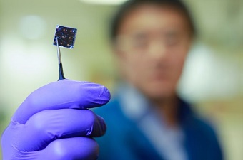
Materials scientists from the UCLA Samueli School of Engineering have developed a highly efficient thin-film solar cell that generates more energy from sunlight than typical solar panels, thanks to its double-layer design.
The device is made by spraying a thin layer of perovskite — an inexpensive compound of lead and iodine that has been shown to be very efficient at capturing energy from sunlight — onto a commercially available solar cell. The solar cell that forms the bottom layer of the device is made of a compound of copper, indium, gallium and selenide, or CIGS.
The team’s new cell converts 22.4% of the incoming energy from the sun, a record in power conversion efficiency for a perovskite–CIGS tandem solar cell. The performance was confirmed in independent tests at the U.S. Department of Energy’s National Renewable Energy Laboratory. (The previous record, set in 2015 by a group at IBM’s Thomas J. Watson Research Center, was 10.9%.) The UCLA device’s efficiency rate is similar to that of the poly-silicon solar cells that currently dominate the photovoltaics market.
“With our tandem solar cell design, we’re drawing energy from two distinct parts of the solar spectrum over the same device area,” Yang said. “This increases the amount of energy generated from sunlight compared to the CIGS layer alone.”
Yang added that the technique of spraying on a layer of perovskite could be easily and inexpensively incorporated into existing solar-cell manufacturing processes.
The cell’s CIGS base layer, which is about 2 microns (or two-thousandths of a millimeter) thick, absorbs sunlight and generates energy at a rate of 18.7% efficiency on its own, but adding the 1 micron-thick perovskite layer improves its efficiency — much like how adding a turbocharger to a car engine can improve its performance. The two layers are joined by a nanoscale interface that the UCLA researchers designed; the interface helps give the device higher voltage, which increases the amount of power it can export.
And the entire assembly sits on a glass substrate that’s about 2 millimeters thick.
“Our technology boosted the existing CIGS solar cell performance by nearly 20% from its original performance,” Yang said. “That means a 20% reduction in energy costs."
He added that devices using the two-layer design could eventually approach 30% power conversion efficiency. That will be the research group’s next goal.
The study’s lead authors are Qifeng Han, a visiting research associate in Yang’s laboratory, and Yao-Tsung Hsieh and Lei Meng, who both recently earned their doctorates at UCLA. The study’s other authors are members of Yang’s research group and researchers from Solar Frontier Corp.’s Atsugi Research Center in Japan.
The research was supported by the National Science Foundation and the Air Force Office of Scientific Research. Yang and his research group have been working on tandem solar cells for several years and their accomplishments include developing transparent tandem solar cells that could be used in windows.
Share on:


Suggested Items
Insulectro’s 'Storekeepers' Extend Their Welcome to Technology Village at IPC APEX EXPO
04/03/2024 | InsulectroInsulectro, the largest distributor of materials for use in the manufacture of PCBs and printed electronics, welcomes attendees to its TECHNOLOGY VILLAGE during this year’s IPC APEX EXPO at the Anaheim Convention Center, April 9-11, 2024.
ENNOVI Introduces a New Flexible Circuit Production Process for Low Voltage Connectivity in EV Battery Cell Contacting Systems
04/03/2024 | PRNewswireENNOVI, a mobility electrification solutions partner, introduces a more advanced and sustainable way of producing flexible circuits for low voltage signals in electric vehicle (EV) battery cell contacting systems.
Heavy Copper PCBs: Bridging the Gap Between Design and Fabrication, Part 1
04/01/2024 | Yash Sutariya, Saturn Electronics ServicesThey call me Sparky. This is due to my talent for getting shocked by a variety of voltages and because I cannot seem to keep my hands out of power control cabinets. While I do not have the time to throw the knife switch to the off position, that doesn’t stop me from sticking screwdrivers into the fuse boxes. In all honesty, I’m lucky to be alive. Fortunately, I also have a talent for building high-voltage heavy copper circuit boards. Since this is where I spend most of my time, I can guide you through some potential design for manufacturability (DFM) hazards you may encounter with heavy copper design.
Trouble in Your Tank: Supporting IC Substrates and Advanced Packaging, Part 5
03/19/2024 | Michael Carano -- Column: Trouble in Your TankDirect metallization systems based on conductive graphite or carbon dispersion are quickly gaining acceptance worldwide. Indeed, the environmental and productivity gains one can achieve with these processes are outstanding. In today’s highly competitive and litigious environment, direct metallization reduces costs associated with compliance, waste treatment, and legal issues related to chemical exposure. What makes these processes leaders in the direct metallization space?
AT&S Shines with Purest Copper on World Recycling Day
03/18/2024 | AT&SThe Styrian microelectronics specialist AT&S is taking World Recycling Day as an opportunity to review the progress that has been made in recent months at its sites around the world in terms of the efficient use of resources: