


 It’s Only Common Sense: OCCAM—the Time Is Now
 Marcy's Musings: The Growing Industry
 Dan’s Biz Bookshelf: Seeing the How
Watching Two-Dimensional Materials Grow
August 31, 2018 | TU WienEstimated reading time: 2 minutes
They are among the thinnest structures on earth: “two dimensional materials” are crystals which consist of only one or a few layers of atoms. They often display unusual properties, promising many new applications in opto-electronics and energy technology. One of these materials is 2D-molybdenum sulphide, an atomically thin layer of molybdenum and sulphur atoms.
The production of such ultra-thin crystals is difficult. The crystallisation process depends on many different factors. In the past, different techniques have yielded quite diverse results, but the reasons for this could not be accurately explained. Thanks to a new method developed by research teams at TU Wien, the University of Vienna and Joanneum Research in Styria, for the first time ever it is now possible to observe the crystallisation process directly under the electron microscope. The method has now been presented in the scientific journal ‘ACS nano’.
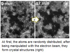
From Gas to Crystal
“Molybdenum sulphide can be used in transparent and flexible solar cells or for sustainably generating hydrogen for energy storage”, says the lead author of the study, Bernhard C. Bayer from the Institute of Materials Chemistry at TU Wien. “In order to do this, however, high-quality crystals must be grown under controlled conditions.”
Usually this is done by starting out with atoms in gaseous form and then condensing them on a surface in a random and unstructured way. In a second step, the atoms are arranged in regular crystal form – through heating, for example. “The diverse chemical reactions during the crystallisation process are, however, still unclear, which makes it very difficult to develop better production methods for 2D materials of this kind”, Bayer states.
Thanks to a new method, however, it should now be possible to accurately study the details of the crystallisation process. “This means it is no longer necessary to experiment through trial and error, but thanks to a deeper understanding of the processes, we can say for certain how to obtain the desired product”, Bayer adds.
Graphene as a Substrate
First, molybdenum and sulphur are placed randomly on a membrane made of graphene. Graphene is probably the best known of the 2D materials – a crystal with a thickness of only one atom layer consisting of carbon atoms arranged in a honeycomb lattice. The randomly arranged molybdenum and sulphur atoms are then manipulated in the electron microscope with a fine electron beam. The same electron beam can be used simultaneously to image the process and to initiate the crystallization process.
That way it has now become possible for the first time to directly observe how the atoms move and rearrange during the growth of the material with a thickness of only two atomic layers. “In doing so, we can see that the most thermodynamically stable configuration doesn't necessarily always have to be the final state”, Bayer says. Different crystal arrangements compete with one another, transform into each other and replace one another. “Therefore, it is now clear why earlier investigations had such varying results. We are dealing with a complex, dynamic process.” The new findings will help to adapt the structure of the 2D materials more precisely to application requirements in future by interfering with the rearrangement processes in a targeted manner.
Share on:


Suggested Items
Groundbreaking Ceremony Marks the Beginning of a New Era for Newccess Industrial; The Construction of the MINGXIN Building
04/12/2024 | Newccess IndustrialOn a clear and sunny day in March, the groundbreaking ceremony for the MINGXIN Building took place in Shenzhen, China. This moment marked the official commencement of construction for a project that will reshape the semiconductor materials industry.
The Need for a Holistic Global Sustainability Standard
04/10/2024 | Michael Ford, Aegis SoftwareNo one can deny that the resources of our fragile planet are finite. The environment seems like a third party, subject to constant degradation. We’re acutely aware of the effects of pollution on our climate, and despite our “throw-away” culture, recycling and recovery of materials has remained relatively expensive, even as we use more energy just to survive.
iNEMI Publishes Four Roadmap Topics
04/04/2024 | iNEMIThe International Electronics Manufacturing Initiative (iNEMI) announces the availability of the first roadmap topics in the new iNEMI Roadmap format. Printed circuit boards, sustainable electronics, smart manufacturing, and mmWave materials and test are now available online.
Insulectro’s 'Storekeepers' Extend Their Welcome to Technology Village at IPC APEX EXPO
04/03/2024 | InsulectroInsulectro, the largest distributor of materials for use in the manufacture of PCBs and printed electronics, welcomes attendees to its TECHNOLOGY VILLAGE during this year’s IPC APEX EXPO at the Anaheim Convention Center, April 9-11, 2024.
Checking In With ICAPE Group
04/03/2024 | Nolan Johnson, I-Connect007ICAPE Group’s field application engineer Erik Pederson drills down on sustainability, supply chain resiliency, and what value engineering really looks like in this exclusive interview. Founded in 1999, European-based ICAPE Group provides 21 million printed circuit boards and over six million technical parts to manufacturers every month. With 30 PCB manufacturing partners globally and 50 partners providing a wide array of technical parts, ICAPE Group has operations in China, Taiwan, Thailand, South Korea, Vietnam, South Africa, Europe, Mexico, and the United States. The company also focuses on the value proposition for its customers.