


 Marcy's Musings: The Growing Industry
 It’s Only Common Sense: Here’s What To Do After IPC APEX EXPO 2024
 Dan’s Biz Bookshelf: Seeing the How
First Truly Black Solar Modules Roll off Industrial Production Line
September 11, 2018 | Aalto UniversityEstimated reading time: 2 minutes
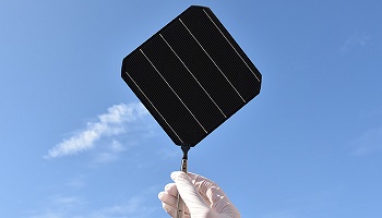
A 2011 invention made by Aalto University’s researchers has proceeded from concept to reality. Just a few years ago, the researchers obtained the record efficiency of 22% in the lab for nanostructured solar cells using atomic layer deposition. Now with the help of industrial partners and joint European collaboration, the first prototype modules have been manufactured on an industrial production line.
'Our timing could not have been better,' Professor Hele Savin, who led the research, was pleased to share. Indeed, 2018 is commonly called the 'Year of Black Silicon' due to its rapid expansion in the photovoltaic (PV) industry. It has enabled the use of diamond-wire sawing in multicrystalline silicon, which reduces costs and environmental impact. However, there is still plenty of room for improvement as the current black silicon used in industry consists of shallow nanostructures that lead to sub-optimal optical properties and require a separate antireflection coating.
Aalto’s approach consists of using deep needle-like nanostructures to make an optically perfect surface that eliminates the need for the antireflection coatings. Their industrial production, however, was not an easy task. 'We were worried that such a fragile structure would not survive the multi-step mass production, because of rough handling by robots or module lamination.'
Luckily, the concerns were proven not to be an issue. The cells and modules were truly black when they came out from production and had no signs of damage. The best module was producing energy with more than 20% efficiency. In addition to excellent optical properties, the researchers were positively surprised that their black cells had additional unexpected benefits, such as a high tolerance towards impurities and much better long-term stability as compared to the industry standard reference cells.
How expensive is black silicon technology? 'Questions related to techno-economical analysis are always difficult, especially for material scientists like us. Luckily, we got help from people with related expertise,“ Savin answers. The project partners provided data to Profesor Joshua Pearce at Michigan Tech University, whose preliminary calculations indicate that, while deep nanostructures are expensive to fabricate, the higher performance of the end product could balance out the total costs, e.g. due to a lower amount of process steps.
The R&D project (BLACK) was part of the Solar-ERANET network and was funded by the EU and Business Finland. The project partners included Spain’s Universitat Politècnica de Catalunya, Germany’s Solar World Innovations GmbH and Finnish-based companies Beneq, Naps Solar Systems, Cencorp, Okmetic, and Fortum. The project key findings will be presented by PhD student Toni Pasanen at the European Photovoltaic Solar Energy Conference in Brussels at the end of September 2018, where he will also receive an award in 'recognition of the most remarkable and outstanding research work in the field of PV'.
Share on:


Suggested Items
Digitalisation and ESG
04/19/2024 | Marina Hornasek-Metzl, AT&SDigitalisation and ESG are prominent and high-priority topics in the global business community. The first focuses on applying technology throughout the value chain to produce faster, smarter, and more desirable business outcomes. The latter emphasises the broader value a business is expected to create for its stakeholders from an environmental, social, and governance perspective.
Real Time with... IPC APEX EXPO 2024: Looking Back, Looking Forward With IEC
04/19/2024 | Real Time with...IPC APEX EXPOIEC came to the RTW booth and discussed both the legacy of IEC's past and the vision for its future. Industry veteran Bruno Ferri highlighted his quarter-century tenure in the industry and with IEC since its founding. He still exhibits boundless enthusiasm for the industry. Brando Stone, a young professional and a future face of IEC, talked about IEC's plans going forward and his experience at this year's IPC APEX EXPO.
Seeking Employment: Meet Parker Capers
04/18/2024 | Barry Matties, I-Connect007Parker Capers, a cybersecurity professional with a decade of experience in the SMT industry, earned a bachelor’s degree from DeVry and is CompTIA Security Plus certified. He is open to various industries but has a strong affinity for manufacturing due to extensive familiarity. Parker appreciates smaller companies where personal connections matter. Are you hiring?
SEMI Applauds CHIPS Program Office Progress to Diversify U.S. Semiconductor Industry Workforce
04/18/2024 | SEMIThe SEMI Foundation, the arm of SEMI dedicated to supporting economic opportunity for workers and the sustained growth of the microelectronics industry by creating pathways and opportunities for job seekers, applauded strides made by the CHIPS Program Office to diversify the U.S. semiconductor industry workforce and its release of the First Annual Report Regarding the Opportunities and Inclusion Activities Undertaken by the Department of Commerce.
VDMA: Machine Vision Navigating Through Uncertain Times
04/18/2024 | VDMAFor over a decade, the European machine vision industry has reported steady growth, with turnover increasing by an average of 9 percent annually between 2012 and 2022. Despite a temporary setback in 2020 (minus 4 percent) due to the Covid-19 pandemic, the industry rebounded strongly in 2021 (plus 17 percent) and 2022 (plus 11 percent).