


 The Right Approach: I Hear the Train A Comin'
 It’s Only Common Sense: OCCAM—the Time Is Now
 Marcy's Musings: The Growing Industry
Spray-On Antennas Could Be the Tech Connector of the Future
September 24, 2018 | Drexel UniversityEstimated reading time: 5 minutes
The promise of wearables, functional fabrics, the Internet of Things, and their “next-generation” technological cohort seems tantalizingly within reach. But researchers in the field will tell you a prime reason for their delayed “arrival” is the problem of seamlessly integrating connection technology — namely, antennas — with shape-shifting and flexible “things.”
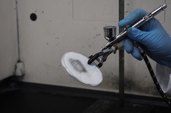
Image caption: Spray-applied MXene antennas could open the door for new applications in smart technology, wearables and IoT devices.
But a breakthrough by researchers in Drexel’s College of Engineering, could now make installing an antenna as easy as applying some bug spray.
In research recently published in Science Advances, the group reports on a method for spraying invisibly thin antennas, made from a type of two-dimensional, metallic material called MXene, that perform as well as those being used in mobile devices, wireless routers and portable transducers.
“This is a very exciting finding because there is a lot of potential for this type of technology,” said Kapil Dandekar, PhD, a professor of Electrical and Computer Engineering in the College of Engineering, who directs the Drexel Wireless Systems Lab, and was a co-author of the research. “The ability to spray an antenna on a flexible substrate or make it optically transparent means that we could have a lot of new places to set up networks — there are new applications and new ways of collecting data that we can’t even imagine at the moment.”
“We found that even transparent antennas with thicknesses of tens of nanometers were able to communicate efficiently,” said Asia Sarycheva, a doctoral candidate in the A.J. Drexel Nanomaterials Institute and Materials Science and Engineering Department. “By increasing the thickness up to 8 microns, the performance of MXene antenna achieved 98 percent of its predicted maximum value.”
Preserving transmission quality in a form this thin is significant because it would allow antennas to easily be embedded — literally, sprayed on — in a wide variety of objects and surfaces without adding additional weight or circuitry or requiring a certain level of rigidity.
Researchers in the College of Engineering developed and tested spray-applied antennas made from a type of two-dimensional material called MXene.
“This technology could enable the truly seamless integration of antennas with everyday objects which will be critical for the emerging Internet of Things,” Dandekar said. “Researchers have done a lot of work with non-traditional materials trying to figure out where manufacturing technology meets system needs, but this technology could make it a lot easier to answer some of the difficult questions we’ve been working on for years.”
Initial testing of the sprayed antennas suggest that they can perform with the same range of quality as current antennas, which are made from familiar metals, like gold, silver, copper and aluminum, but are much thicker than MXene antennas. Making antennas smaller and lighter has long been a goal of materials scientists and electrical engineers, so this discovery is a sizable step forward both in terms of reducing their footprint as well as broadening their application.
“Current fabrication methods of metals cannot make antennas thin enough and applicable to any surface, in spite of decades of research and development to improve the performance of metal antennas,” said Yury Gogotsi, PhD, Distinguished University and Bach professor of Materials Science and Engineering in the College of Engineering, and Director of the A.J. Drexel Nanomaterials Institute, who initiated and led the project. “We were looking for two-dimensional nanomaterials, which have sheet thickness about hundred thousand times thinner than a human hair; just a few atoms across, and can self-assemble into conductive films upon deposition on any surface. Therefore, we selected MXene, which is a two-dimensional titanium carbide material, that is stronger than metals and is metallically conductive, as a candidate for ultra-thin antennas.”
Drexel researchers discovered the family of MXene materials in 2011 and have been gaining an understanding of their properties, and considering their possible applications, ever since. The layered two-dimensional material, which is made by wet chemical processing, has already shown potential in energy storage devices, electromagnetic shielding, water filtration, chemical sensing, structural reinforcement and gas separation.
Naturally MXene materials have drawn comparisons to promising two-dimensional materials like graphene, which won the Nobel Prize in 2010 and has been explored as a material for printable antennas. In the paper, the Drexel researchers put the spray-on antennas up against a variety of antennas made from these new materials, including graphene, silver ink and carbon nanotubes. The MXene antennas were 50 times better than graphene and 300 times better than silver ink antennas in terms of preserving the quality of radio wave transmission.
“The MXene antenna not only outperformed the macro and micro world of metal antennas, we went beyond the performance of available nanomaterial antennas, while keeping the antenna thickness very low,” said Babak Anasori, PhD, a research assistant professor in A.J. Drexel Nanomaterials Institute. “The thinnest antenna was as thin as 62 nanometers — about thousand times thinner than a sheep of paper — and it was almost transparent. Unlike other nanomaterials fabrication methods, that requires additives, called binders, and extra steps of heating to sinter the nanoparticles together, we made antennas in a single step by airbrush spraying our water-based MXene ink.”
The group initially tested the spray-on application of the antenna ink on a rough substrate — cellulose paper — and a smooth one — polyethylene terephthalate sheets — the next step for their work will be looking at the best ways to apply it to a wide variety of surfaces from glass to yarn and skin.
“Further research on using materials from the MXene family in wireless communication may enable fully transparent electronics and greatly improved wearable devices that will support the active lifestyles we are living,” Anasori said.
Share on:


Suggested Items
Designer’s Notebook: What Designers Need to Know About Manufacturing, Part 2
04/24/2024 | Vern Solberg -- Column: Designer's NotebookThe printed circuit board (PCB) is the primary base element for providing the interconnect platform for mounting and electrically joining electronic components. When assessing PCB design complexity, first consider the component area and board area ratio. If the surface area for the component interface is restricted, it may justify adopting multilayer or multilayer sequential buildup (SBU) PCB fabrication to enable a more efficient sub-surface circuit interconnect.
Insulectro’s 'Storekeepers' Extend Their Welcome to Technology Village at IPC APEX EXPO
04/03/2024 | InsulectroInsulectro, the largest distributor of materials for use in the manufacture of PCBs and printed electronics, welcomes attendees to its TECHNOLOGY VILLAGE during this year’s IPC APEX EXPO at the Anaheim Convention Center, April 9-11, 2024.
ENNOVI Introduces a New Flexible Circuit Production Process for Low Voltage Connectivity in EV Battery Cell Contacting Systems
04/03/2024 | PRNewswireENNOVI, a mobility electrification solutions partner, introduces a more advanced and sustainable way of producing flexible circuits for low voltage signals in electric vehicle (EV) battery cell contacting systems.
Heavy Copper PCBs: Bridging the Gap Between Design and Fabrication, Part 1
04/01/2024 | Yash Sutariya, Saturn Electronics ServicesThey call me Sparky. This is due to my talent for getting shocked by a variety of voltages and because I cannot seem to keep my hands out of power control cabinets. While I do not have the time to throw the knife switch to the off position, that doesn’t stop me from sticking screwdrivers into the fuse boxes. In all honesty, I’m lucky to be alive. Fortunately, I also have a talent for building high-voltage heavy copper circuit boards. Since this is where I spend most of my time, I can guide you through some potential design for manufacturability (DFM) hazards you may encounter with heavy copper design.
Trouble in Your Tank: Supporting IC Substrates and Advanced Packaging, Part 5
03/19/2024 | Michael Carano -- Column: Trouble in Your TankDirect metallization systems based on conductive graphite or carbon dispersion are quickly gaining acceptance worldwide. Indeed, the environmental and productivity gains one can achieve with these processes are outstanding. In today’s highly competitive and litigious environment, direct metallization reduces costs associated with compliance, waste treatment, and legal issues related to chemical exposure. What makes these processes leaders in the direct metallization space?