


 The Right Approach: I Hear the Train A Comin'
 It’s Only Common Sense: OCCAM—the Time Is Now
 Marcy's Musings: The Growing Industry
Small Modulator for Big Data
September 25, 2018 | Harvard UniversityEstimated reading time: 3 minutes
Conventional lithium niobite modulators, the longtime workhorse of the optoelectronic industry, may soon go the way of the vacuum tube and floppy disc. Researchers from the Harvard John A. Paulson School of Engineering and Applied Sciences have developed a new method to fabricate and design integrated, on-chip modulators 100 times smaller and 20 times more efficient than current lithium niobite (LN) modulators.
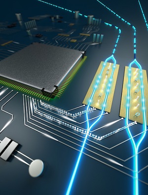
Image Caption: Fiber-optical networks, the backbone of the internet, rely on high-fidelity information conversion from electrical to the optical domain. The researchers combined the best optical material with innovative nanofabrication and design approaches, to realize, energy-efficient, high-speed, low-loss, electro-optic converters for quantum and classical communications (Image courtesy of Second Bay Studios/Harvard SEAS).
“This research demonstrates a fundamental technological breakthrough in integrated photonics,” said Marko Loncar, the Tiantsai Lin Professor of Electrical Engineering at SEAS and senior author of the paper. “Our platform could lead to large-scale, very fast and ultra-low-loss photonic circuits, enabling a wide range of applications for future quantum and classical photonic communication and computation.”
Harvard’s Office of Technology Development (OTD) has worked closely with the Loncar Lab on the formation of a startup company, HyperLight, that intends to commercialize a portfolio of foundational intellectual property related to this research. Readying the technology toward the launch of HyperLight has been aided by funding from OTD’s Physical Sciences & Engineering Accelerator, which provides translational funding for research projects that show potential for significant commercial impact.
Conventional lithium niobite modulators [right] are the backbone of modern telecommunications but are bulky, expensive and power hungry. This integrated, on-chip modulator [center] is 100 times smaller and 20 times more efficient. (Image courtesy of the Loncar Lab/ Harvard SEAS)
Lithium niobate modulators are the backbone of modern telecommunications, converting electronic data to optical information in fiber optic cables. However, conventional LN modulators are bulky, expensive and power hungry. These modulators require a drive voltage of 3 to 5 volts, significantly higher than that provided by typical CMOS circuitry, which provides about 1 volt. As a result, separate, power-consuming amplifiers are needed to drive the modulators, severely limiting chip-scale optoelectronic integration.
“We show that by integrating lithium niobate on a small chip, the drive voltage can be reduced to a CMOS-compatible level,” said Cheng Wang, co-first author of the paper, former PhD student and postdoctoral fellow at SEAS, and currently Assistant Professor at City University of Hong Kong. “Remarkably, these tiny modulators can also support data transmission rates up to 210 Gbit/s. It’s like Antman – smaller, faster and better.”
“Highly-integrated yet high-performance optical modulators are very important for the closer integration of optics and digital electronics, paving the way towards future fiber-in-fiber-out opto-electronic processing engines,” said Peter Winzer, Director of Optical Transmission Research at Nokia Bell Labs, the industrial partner in this project, and coauthor of the paper. “We see this new modulator technology as a promising candidate for such solutions.”
Lithium niobite is considered by many in the field to be difficult to work with on small scales, an obstacle that has so far ruled out practical integrated, on-chip applications. In previous research, Loncar and his team demonstrated a technique to fabricate high-performance lithium niobate microstructures using standard plasma etching to physically sculpt microresonators in thin lithium niobate films.
Combining that technique with specially designed electrical components, the researchers can now design and fabricate an integrated, high-performance on-chip modulator.
“Previously, if you wanted to make modulators smaller and more integrated, you had to compromise their performance,” said Mian Zhang, a postdoctoral fellow at SEAS and co-first author of the research. “For example, existing integrated modulators can easily lose the majority of the light as it propagates on the chip. In contrast, we have reduced losses by more than an order of magnitude. Essentially, we can control light without losing it.”
“Because a modulator is such a fundamental component of communication technology — with a role equivalent to that of a transistor in computation technology — the applications are enormous,” said Zhang. “The fact that these modulators can be integrated with other components on the same platform could provide practical solutions for next-generation long-distance optical networks, data center optical interconnects, wireless communications, radar, sensing and so on.”
This research was co-authored by Xi Chen, Maxime Bertrand, Amirhassan Shams-Ansari, and Sethumadhavan Chandrasekhar.
It was supported in part by National Science Foundation and the Harvard University Office of Technology Development’s Physical Sciences and Engineering Accelerator Award. Device fabrication was performed at the Harvard University Center for Nanoscale Systems (CNS), a member of the National Nanotechnology Coordinated Infrastructure Network (NNCI), which is supported by the National Science Foundation.
Share on:


Suggested Items
Warm Windows and Streamlined Skin Patches – IDTechEx Explores Flexible and Printed Electronics
04/26/2024 | IDTechExFlexible and printed electronics can be integrated into cars and homes to create modern aesthetics that are beneficial and easy to use. From luminous car controls to food labels that communicate the quality of food, the uses of this technology are endless and can upgrade many areas of everyday life.
iNEMI Packaging Tech Topic Series: Role of EDA in Advanced Semiconductor Packaging
04/26/2024 | iNEMIAdvanced semiconductor packaging with heterogenous integration has made on-package integration of multiple chips a crucial part of finding alternatives to transistor scaling. Historically, EDA tools for front-end and back-end design have evolved separately; however, design complexity and the increased number of die-to-die or die-to-substrate interconnections has led to the need for EDA tools that can support integration of overall design planning, implementation, and system analysis in a single cockpit.
Koh Young Showcases Award-winning Inspection Solutions at SMTconnect with SmartRep in Hall 4A.225
04/25/2024 | Koh Young TechnologyKoh Young Technology, the industry leader in True 3D measurement-based inspection solutions, will showcase an array of award-winning inspection and measurement solutions at SMTconnect alongside its sales partner, SmartRep, in booth 4A.225 at NürnbergMesse from June 11-13, 2023. The following offers a glimpse into what Koh Young will present at the tradeshow:
Real Time with… IPC APEX EXPO 2024: Plasmatreat: Innovative Surface Preparation Solutions
04/25/2024 | Real Time with...IPC APEX EXPOIn this interview, Editor Nolan Johnson speaks with Hardev Grewal, CEO and president of Plasmatreat, a developer of atmospheric plasma solutions. Plasmatreat uses clean compressed air and electricity to create plasma, offering environmentally friendly methods for surface preparation. Their technology measures plasma density for process optimization and can remove organic micro-contamination. Nolan and Hardev also discuss REDOX-Tool, a new technology for removing metal oxides.
Nanotechnology Market to Surpass $53.51 Billion by 2031
04/25/2024 | PRNewswireSkyQuest projects that the nanotechnology market will attain a value of USD 53.51 billion by 2031, with a CAGR of 36.4% over the forecast period (2024-2031).