


 It’s Only Common Sense: OCCAM—the Time Is Now
 Marcy's Musings: The Growing Industry
 Dan’s Biz Bookshelf: Seeing the How
Thin Films for More Efficient Solar Cells
October 8, 2018 | KAUSTEstimated reading time: 2 minutes
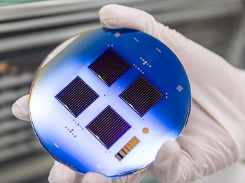
The efficiency of solar cells can be increased by thin-film contacts developed by researchers at KAUST.
A silicon solar cell that uses an electron-selective tantalum-nitride-metal contact for improved efficiency.
Improving the performance of solar cells requires scrutinizing every aspect of their design. First, this means improving the crystalline quality of the absorbing material to maximize the conversion of photons to negatively charged electrons and positively charged holes. Next, the device’s architecture must be optimized to ensure these charge carriers can move efficiently through the material. Finally, the electrical contacts that extract the carriers from the device and into an external circuit need to be perfected.
Xinbo Yang and his colleagues from the KAUST Solar Center and the KAUST Core Lab, together with coworkers from the Australian National University, focus on this third step by developing electron-selective tantalum-nitride thin-film contacts for silicon solar cells.
The interface between a silicon and a metal contact can create a high-resistance barrier that disrupts current flow. Additionally, the metal-induced electronic states at the surface of silicon enable the charge carrier to recombine, which reduces the conversion efficiency. Traditionally, high-cost processes, such as diffusion and chemical-vapor deposition of additional layers were adopted to reduce the contact resistance and carrier recombination.
The team led by Stefaan De Wolf (left) and Xinbo Yang (right) created a silicon solar cell that used an electron-selective tantalum-nitride-metal contact that improved the power conversion efficiency.
Yang and the team combat these problems by placing tantalum nitride on silicon using a method known as atomic-layer deposition: they do this by exposing the surface to a gas, causing a high-quality thin film to build up one atom at a time.
“Electron-selective tantalum-nitride contacts can simultaneously reduce the charge carrier recombination and contact resistance,” explains Yang. “This can simplify the complexity of fabricating the device and lower the production cost.”
By experimentally investigating the electrical properties of the tantalum nitride–silicon interface, the researchers showed that the tantalum nitride interlayer was able to reduce the contact resistance to the flow of electrons from silicon and metal contacts made of silver or aluminum. But, it simultaneously blocked the flow of holes, reducing the carrier recombination
The team created a silicon solar cell that used an electron-selective tantalum-nitride-metal contact. They showed that this improved the power conversion efficiency—the ratio between electrical power out to optical power in—by more than 20 percent over a control device built without the tantalum nitride. They also found that it simplified the device fabrication sequence, and cost, by eliminating doping and contact opening processes.
“We are also investigating the potential application of tantalum nitride electron transport layers for organic and perovskite solar cells,” explain KAUST scientist and principal investigator, Stefaan De Wolf.
Share on:


Suggested Items
Water Management in a Large Printed Circuit Board Manufacturer
04/15/2024 | Charles Nehrig, TTM TechnologiesTTM’s environmental management is grounded in its Environmental Statement and Environmental Policy, which promote measures that make for a more responsible environmental management process. Our management system helps TTM work toward minimizing its environmental footprint and increasing the sustainability of its operations. TTM monitors its environmental performance just as it monitors its operational performance, and provides the resources required to adhere to the Company’s environmental responsibilities.
Happy’s Tech Talk #27: Integrated Mesh Power System (IMPS) for PCBs
04/08/2024 | Happy Holden -- Column: Happy’s Tech TalkA significant decrease in HDI substrate production cost can be achieved by reducing the number of substrate layers from conventional through-hole multilayers and microvia multilayers of eight, 10, 12, and more to only two layers. Besides reducing direct processing steps, the yield will increase as defect-producing operations are eliminated. The integrated mesh power system (IMPS) was invented in the latter years of MCM-D use for thin-film fabrication. Those geometries fit today into our use of ultra HDI.
Trouble in Your Tank: Supporting IC Substrates and Advanced Packaging, Part 5
03/19/2024 | Michael Carano -- Column: Trouble in Your TankDirect metallization systems based on conductive graphite or carbon dispersion are quickly gaining acceptance worldwide. Indeed, the environmental and productivity gains one can achieve with these processes are outstanding. In today’s highly competitive and litigious environment, direct metallization reduces costs associated with compliance, waste treatment, and legal issues related to chemical exposure. What makes these processes leaders in the direct metallization space?
Indium Corporation Experts to Present at SEMI THERM
03/07/2024 | Indium CorporationIndium Corporation Global Account Manager and Senior Thermal Technologist Tim Jensen and Product Development Specialist for Thermal Interface Materials Miloš Lazić will present on thermal interface material (TIM) technology at SEMI-THERM, taking place March 25–28 in San Jose, California, U.S.
Indium Corporation to Showcase Proven EV Products and High-Reliability Alloys at Productronica China
02/28/2024 | Indium CorporationAs a materials pioneer and trusted partner in electric vehicle (EV) and e-Mobility manufacturing, Indium Corporation is proud to showcase its high-reliability alloys and soldering solutions at Productronica China, March 20-22, in Shanghai.