


 The Right Approach: I Hear the Train A Comin'
 It’s Only Common Sense: OCCAM—the Time Is Now
 Marcy's Musings: The Growing Industry
Special Deformation of Nanotubes to Allow them to Change Conductivity
October 23, 2018 | NUST MISISEstimated reading time: 3 minutes
Scientists from the NUST MISIS Laboratory of Inorganic Nanomaterials together with their international colleagues have proved it possible to change the structural and conductive properties of nanotubes by stretching them. This can potentially expand nanotubes’ application into electronics and high-precision sensors such as microprocessors and high-precision detectors. The research article has been published in Ultramicroscopy.
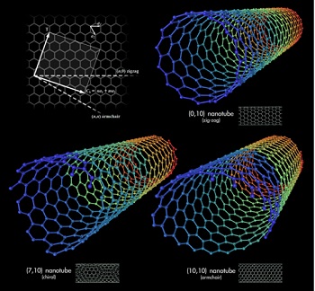
Figure 1: Different types of nanotubes: 1) zigzag, 2) chiral and 3) armchair (or dentated).
Carbon nanotubes can be represented as a sheet of graphene rolled in a special way. There are different ways of “folding” it, which leads to the graphene edges interconnecting at different angles, forming either armchair, zigzag or chiral nanotubes.
Nanotubes are considered to be promising materials for use in electronics and sensors because they have high electrical conductivity, which would work well in things like microprocessors and high-precision detectors. However, when producing carbon nanotubes, it is hard to control their conductivity. Nanotubes with metallic and semiconducting properties can grow into a single array while microprocessor-based electronics require semiconducting nanotubes that have the same characteristics.
Scientists from the NUST MISIS Laboratory of Inorganic Nanomaterials jointly with a research team from Japan, China and Australia, led by Professor Dmitri Golberg, have proposed a method that allows for the modification of the structure of ready-made nanotubes and thus changes their conductive properties.
“The basis of the nanotube — a folded layer of graphene — is a grid of regular hexagons, the vertices of which are carbon atoms. If one of the carbon bonds in the nanotube is rotated by 90° degrees, a pentagon and a heptagon are formed at this [junction] instead of a hexagon, and a so-called Stone-Wales defect is obtained in this case. Such a defect can occur in the structure under certain conditions. Back in the late 90s, it was predicted that the migration of this defect along the walls of a highly heated nanotube with the application of mechanical stress could lead to a change in its structure — a sequential change in the chirality of the nanotube, which leads to a change in its electronic properties. No experimental evidence for this hypothesis has previously been obtained, but our research paper has presented convincing proof of it”, said Associate Professor Pavel Sorokin, Doctor of Physical & Mathematical Sciences and head of the “Theoretical Materials Science of Nanostructures” infrastructure project at the NUST MISIS Laboratory of Inorganic Nanomaterials.
*Scientists from the NUST MISIS Laboratory of Inorganic Nanomaterials have conducted simulations of the experiment at the atomic level. At first, the nanotubes were lengthened to form the first structural defect consisting of two pentagons and two heptagons (a Stone-Wales defect, pic.2a), where the prolonged lengthening of the tube began to “spread” to the sides, rearranging other carbon bonds It was at this stage that the structure of the nanotubes changed. With further stretching, more and more Stone-Wales defects began to form, eventually leading to a change in the nanotubes’ conductivity.
Figure 2: The process of the nanotube structure changing: а) stretching with the first defect formation; b) the restructuring of related carbon bonds; с) the formation of new defects and the continuation of the restructuring of links.
“We were responsible for the theoretical modeling of the process on a supercomputer in the NUST MISIS Laboratory for Modeling and Development of New Materials for the experimental part of the work. We are glad that the simulation results [support] the experimental data”, added Dmitry Kvashnin, co-author of the research work, Candidate of Physical & Mathematical Sciences and a researcher at the NUST MISIS Laboratory of Inorganic Nanomaterials.
The proposed technology is capable of helping in the transformation of “metallic” nanotubes’ structure for their further application in semiconductor electronics and sensors such as microprocessors and ultrasensitive detectors.
Share on:


Suggested Items
Ansys, TSMC Enable a Multiphysics Platform for Optics and Photonics, Addressing Needs of AI, HPC Silicon Systems
04/25/2024 | PRNewswireAnsys announced a collaboration with TSMC on multiphysics software for TSMC's Compact Universal Photonic Engines (COUPE). COUPE is a cutting-edge Silicon Photonics (SiPh) integration system and Co-Packaged Optics platform that mitigates coupling loss while significantly accelerating chip-to-chip and machine-to-machine communication.
T-Global Technology Offers Solutions for Thermal Management Challenges
04/10/2024 | I-Connect007 Editorial TeamJames Hopkins from T-Global discusses the company's focus on thermal management products, including thermal interface materials, heat sinks, and thermal simulation services. He highlights the importance of collaborating with mechanical engineers and addressing challenges in balancing thermal performance and mechanical requirements. Hopkins also mentions the role of thermal simulation in guiding product recommendations and the significance of early collaboration among stakeholders for optimal product outcomes.
The Exploration Company Leverages Ansys to Promote Sustainability in Space
04/05/2024 | ANSYSSpace logistics startup The Exploration Company is advancing sustainable space exploration by leveraging Ansys simulation solutions to develop its modular and reusable space vehicle, Nyx.
Ansys Forms OEM Partnership with SynMatrix to Accelerate RF Filter Design
04/01/2024 | ANSYSAnsys announced a new OEM partnership with SynMatrix to streamline RF filter design workflows for wireless communications applications. SynMatrix develops industry-leading RF filter design and optimization tools that integrate with HFSS electromagnetic simulation.
Altair SimSolid Transforms Simulation for Electronics Industry
03/29/2024 | AltairAltair, a global leader in computational intelligence, announced the upcoming release of Altair SimSolid for electronics, bringing game-changing fast, easy, and precise multi-physics scenario exploration for electronics, from chips, PCBs, and ICs to full system design.