


 Marcy's Musings: The Growing Industry
 It’s Only Common Sense: Here’s What To Do After IPC APEX EXPO 2024
 Dan’s Biz Bookshelf: Seeing the How
Nanocrystals Arrange to Improve Electronics
October 26, 2018 | Lawrence Livermore National LaboratoryEstimated reading time: 2 minutes
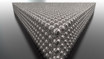
Lawrence Livermore National Laboratory (LLNL) researchers are working to make better electronic devices by delving into the way nanocrystals are arranged inside of them.
Nanocrystals are promising building blocks for new and improved electronic devices, due to their size-tunable properties and ability to integrate into devices at low-cost.
While the structure of nanocrystals has been extensively studied, no one has been able to watch the full assembly process.
That’s where LLNL scientists Christine Orme, Yixuan Yu, Babak Sadigh and a colleague from the University of California, Los Angeles come in.
‘We think the situation can be improved if detailed quantitative information on the nanocrystal assembly process could be identified and if the crystallization process were better controlled,” said Orme, an LLNL material scientist and corresponding author of a paper appearing in the journal Nature Communications.
Nanocrystals inside devices form ensembles, whose collective physical properties, such as charge carrier mobility, depend on both the properties of individual nanocrystals and the way they are arranged. In principle, ordered nanocrystal ensembles, or superlattices, allow for more control in charge transport by facilitating the formation of minibands. However, in practice, few devices built from ordered nanocrystal superlattices are on the market.
Most previous studies use solution evaporation methods to generate nanocrystal superlattices and probe the assembly process as the solvent is being gradually removed. It is difficult to obtain quantitative information on the assembly process, however, because the volume and shape of the nanocrystal solution is continually changing in an uncontrollable manner and the capillary forces can drive nanocrystal motion during drying.
Electric field-driven growth offers a solution to this problem. “We have recently demonstrated that an electric field can be used to drive the assembly of well-ordered, 3D nanocrystal superlattices,” Orme said.
Because the electric field increases the local concentration without changing the volume, shape or composition of nanocrystal solution, the crystallizing system can be probed quantitatively without complications associated with capillary forces or scattering from drying interfaces.
As anticipated, the team found that the electric field drives nanocrystals toward the surface, creating a concentration gradient that leads to nucleation and growth of superlattices. Surprisingly, the field also sorts the particles according to size. In essence, the electric field both concentrates and purifies the nanocrystal solution during growth.
“Because of this size sorting effect, the superlattice crystals are better ordered and the size of the nanocrystals in the lattice can be tuned during growth,” Orme said. “This might be a useful tool for optoelectronic devices. We’re working on infrared detectors now and think it might be an interesting strategy for improving color in monitors.”
Share on:


Suggested Items
IMAPS & IPC to Host Onshoring Workshop
04/16/2024 | IPCThe International Microelectronics Assembly and Packaging Society (IMAPS) and IPC will host an Onshoring Workshop to discuss ongoing progress and forward-looking strategies to drive the Onshoring Advanced Packaging and Assembly, April 29 – May 1, 2024, in Arlington, Virginia.
IPC WinterCom 2024 Through the Eyes of One Dedicated Student
04/12/2024 | Sanjay Huprikar, IPCLauriane Testuz stands as a testament to the power of curiosity, perseverance, and the relentless pursuit of knowledge. Her story serves as a reminder that the path to success is often paved by an unwavering commitment to one's dreams.
2023: Year of Extremes for VDL Groep
04/08/2024 | VDL GroepThe year 2023 showed us two sides, with highs and lows. Low points were the passing of Wim van der Leegte in November, the reduction in the number of employees at VDL Nedcar and headwind in the Buses & Coaches division.
IPC, First and Only Organization in the Electronics Industry to Earn ANSI/ANAB Accreditation for Its Workforce Training
04/02/2024 | IPCIPC, the global leader in electronics education, announces a landmark achievement in professional education and training. Ten of IPC’s critical workforce training programs have been accredited by the ANSI National Accreditation Board (ANAB) under the stringent requirements of ANSI/ASTM E2659-18, Standard Practice for Certificate Programs.
Nolan’s Notes: Do More, Get More
04/02/2024 | Nolan Johnson -- Column: Nolan's NotesThis month in SMT007 Magazine, we’re investigating box build, a manufacturing sector so closely adjacent to board assembly that some OEM customers they’re the same thing. To those of us doing this work, we know they’re very different. Traditional electronic assembly work is typically concerned only with attaching the components to the circuit board. That’s our idea of a “finished good.”