


 It’s Only Common Sense: OCCAM—the Time Is Now
 Marcy's Musings: The Growing Industry
 Dan’s Biz Bookshelf: Seeing the How
Scientists Obtain New Class of Curved Beams for Biosensors and Nanoparticle Control
October 26, 2018 | Tomsk Polytechnic UniversityEstimated reading time: 2 minutes
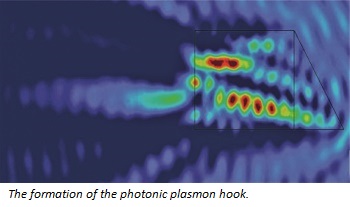
A new class of curved plasmon beams named as a photonic hook plasmon was obtained by researchers from Tomsk Polytechnic University and the Institute of Ultra High-Frequency Semiconductor Electronics of the Russian Academy of Sciences. Due to their small size, they can be used as a nanoparticle manipulator, as well as in biosensors to study substances in small volumes and plasmon microscopes for benefiting superresolution. The findings of the study were published in Annalen der Physik.
A plasmon is a quasi-particle that occurs in solids or near their surface due to electron oscillations. Surface plasmons interact strongly with light; therefore, they determine certain optical properties of metals. Since 2007, scientists have known the only type of curvilinear plasmon waves occurring on the surface of metals, i.e. the Airy rays and their derivatives.
"I should mention that the formation of curvilinear plasmon hooks has so far been possible only on the basis of the Airy family that requires a rather sophisticated and time-consuming method.
We proposed a new class of curved surface plasmon wave, the photonic hook plasmon (PHP), which is fundamentally simpler to generate and has the curvature of beams close to the size of the plasmon wavelength. It is based on the interaction of the surface plasmon wave with a dielectric layer of a special non-symmetric form," says a leader of the project, TPU Professor Igor V. Minin from the Division of Electronic Engineering.
The search of principles to create novel curved beams is an exciting modern field of research that is opening wide fundamental and practical prospects.
In the study, the authors used dielectric particles, e.g. fluoroplastic, with a size of two wavelengths, located on a metal surface. One side of the particle is made in the form of a prism and the second is a square. As the researchers note, particles of different forms can also be used to generate a photonic plasmon hook.
“A flat plasmon wave falls on the conical part of the dielectric, passes through the particle and on the back, square side a focused curvilinear region appears. In shape, it is similar to a hook. Earlier, we successfully used this method for photons and now we demonstrated that the method is appropriate to plasmons too,” clarifies Igor Minin.
The obtained photonic plasmon hook has an important advantage over the Airy rays, i.e. it is much smaller. The curvature of beams is close to the size of the plasmon wavelength, which represents the smallest radius of curvature ever recorded for the SPP beam and makes it possible to use it at the nanoscale.
"In practice such plasmon beams are of interest for biomedical applications, e.g. for biosensors and the synthesis of advanced materials, devices for optical manipulation, e.g. for switching optical signals, and for obtaining new molecules because the ‘hook’ due to its properties can bring together atoms of different elements and much more. This area of research is just in the very beginning of its long journey," says the scientist.
Share on:


Suggested Items
Designer’s Notebook: What Designers Need to Know About Manufacturing, Part 2
04/24/2024 | Vern Solberg -- Column: Designer's NotebookThe printed circuit board (PCB) is the primary base element for providing the interconnect platform for mounting and electrically joining electronic components. When assessing PCB design complexity, first consider the component area and board area ratio. If the surface area for the component interface is restricted, it may justify adopting multilayer or multilayer sequential buildup (SBU) PCB fabrication to enable a more efficient sub-surface circuit interconnect.
IDTechEx Report Unveils 3D Electronics Status and Opportunities
04/22/2024 | PRNewswire3D electronics is an emerging manufacturing approach that enables electronics to be integrated within or onto the surface of objects. 3D electronic manufacturing techniques empower new features, including mass customizability, greater integration, and improved sustainability in the electronics industry.
NASA, Japan Advance Space Cooperation, Sign Agreement for Lunar Rover
04/11/2024 | NASANASA Administrator Bill Nelson and Japan’s Minister of Education, Culture, Sports, Science and Technology (MEXT) Masahito Moriyama have signed an agreement to advance sustainable human exploration of the Moon.
Lockheed Martin Conducts Historic LRASM Flight Test
04/04/2024 | Lockheed MartinThe U.S. Navy in partnership with Lockheed Martin [NYSE: LMT] successfully conducted a historic Long-Range Anti-Ship Missile (LRASM) flight test with four missiles simultaneously in flight.
Ynvisible Appoints Felix Karlsson as Director
04/02/2024 | Ynvisible Interactive Inc.Ynvisible Interactive Inc. is pleased to announce the appointment of Felix Karlsson as a Director of the Company effective immediately.