


 It’s Only Common Sense: OCCAM—the Time Is Now
 Marcy's Musings: The Growing Industry
 Dan’s Biz Bookshelf: Seeing the How
Detecting Light in a Different Dimension
November 14, 2018 | Brookhaven National LaboratoryEstimated reading time: 3 minutes
Scientists from the Center for Functional Nanomaterials (CFN)—a U.S. Department of Energy (DOE) Office of Science User Facility at Brookhaven National Laboratory—have dramatically improved the response of graphene to light through self-assembling wire-like nanostructures that conduct electricity.
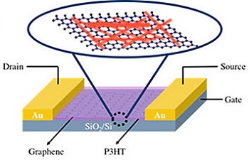
Image Caption: Cartoon of the graphene-P3HT nanowire hybrid field-effect transistor. Placing the nanowire mesh (red) on top of the graphene (purple) improves the device's response to light. The silicon dioxide/silicon (grey) substrate, or "gate" electrode, controls the flow of electrical current between the electron source and drain (in this case, Au, or gold, electrodes). The scientists used electron-beam lithography to pattern the device.
The improvement could pave the way for the development of graphene-based detectors that can quickly sense light at very low levels, such as those found in medical imaging, radiation detection, and surveillance applications.
Graphene is a two-dimensional (2-D) nanomaterial with unusual and useful mechanical, optical, and electronic properties. It is both extremely thin and incredibly strong, detects light of almost any color, and conducts heat and electricity well. However, because graphene is made of sheets of carbon only one atom thick, it can only absorb a very small amount of incoming light (about two percent).
One approach to overcoming this problem is to combine graphene with strong light-absorbing materials, such as organic compounds that conduct electricity. Scientists recently demonstrated an improved photoresponse by placing thin films (a few tens of nanometers) of one such conductive polymer, poly(3-hexylthiophene), or P3HT, on top of a single layer of graphene.
Now, the CFN scientists have improved the photoresponse by an additional 600% by changing the morphology (structure) of the polymer. Instead of thin films, they used a mesh of nanowires—nanostructures that are many times longer than they are wide—made of the same polymer and similar thickness. The research is described in an article published online on Oct. 12 in ACS Photonics, a journal of the American Chemical Society (ACS).
“We used self-assembly, a very simple and reproducible method, to create the nanowire mesh,” said first author Mingxing Li, a research associate in the CFN Soft and Bio Nanomaterials Group. “Placed in an appropriate solution and stirred overnight, the polymer will form into wire-like nanostructures on its own. We then spin-casted the resulting nanowires onto electrical devices called graphene field-effect transistors (FETs).”
The scientists fabricated FETs made of graphene only, graphene and P3HT thin films, and graphene and P3HT nanowires. After checking the thickness and crystal structure of the FET devices through atomic force microscopy, Raman spectroscopy, and x-ray scattering techniques, they measured their light-induced electrical properties (photoresponsivity). Their measurements of the electric current flowing through the FETs under various light illumination powers revealed that the nanowire FETs improve photoresponse by 600 percent compared to the thin film FETs and 3000 percent compared to graphene-only FETs.
"We did not expect to see such a dramatic improvement just by changing the morphology of the polymer," said co-corresponding author Mircea Cotlet, a materials scientist in the CFN Soft and Bio Nanomaterials Group.
The scientists believe that there are two explanations behind their observations.
“At a certain polymer concentration, the nanowires have dimensions comparable to the wavelength of light,” said Li. “This size similarity has the effect of increasing light scattering and absorption. In addition, crystallization of P3HT molecules within the nanowires provides more charge carriers to transfer electricity to the graphene layer.”
“In contrast to conventional thin films where polymer chains and crystals are mostly randomly oriented, the nanoscale dimension of the wires forces the polymer chains and crystals into a specific orientation, enhancing both light absorption and charge transfer,” said co-author Dmytro Nykyphanchuck, a materials scientist in the CFN Soft and Bio Nanomaterials Group.
The scientists have filed a U.S. patent for their fabrication process, and they are excited to explore light-matter interactions in other 2-D—as well as 0-D and 1-D—materials.
“Plasmonics and nanophotonics—the study of light at the nanometer scale—are emerging research areas,” said Cotlet, who earlier this year co-organized a workshop for user communities of the CFN and the National Synchrotron Light Source II (NSLS-II)—another DOE Office of Science User Facility at Brookhaven—to explore frontiers in these areas. “Nanostructures can manipulate and control light at the nanoscale in very interesting ways. The advanced nanofabrication and nanocharacterization tools at the CFN and NSLS-II are perfectly suited for creating and studying materials with enhanced optoeletronic properties.”
About Brookhaven National Laboratory
Brookhaven National Laboratory is supported by the Office of Science of the U.S. Department of Energy. The Office of Science is the single largest supporter of basic research in the physical sciences in the United States, and is working to address some of the most pressing challenges of our time.
Share on:


Suggested Items
Inkjet Solder Mask ‘Has Arrived’
04/10/2024 | Pete Starkey, I-Connect007I was delighted to be invited to attend an interactive webinar entitled “Solder Mask Coating Made Easy with Additive Manufacturing,” hosted by SUSS MicroTec Netherlands in Eindhoven. The webinar was introduced and moderated by André Bodegom, managing director at Adeon Technologies, and the speakers were Mariana Van Dam, senior product manager PCB imaging solutions at AGFA in Belgium; Ashley Steers, sales manager at Electra Polymers in the UK; and Dr. Luca Gautero, product manager at SUSS MicroTec Netherlands.
NetVia Group Acquires Direct Imaging from Mivatek
04/09/2024 | Miva TechnologiesMiva Technologies is pleased to announce NetVia Group, Irving, TX has acquired a new Miva 2400NG Dual Tray Direct Imaging System with 30-micron capabilities for inner, outer and soldermask imaging.
Teledyne to Acquire Adimec
02/13/2024 | TeledyneTeledyne Technologies Incorporated announced that it has entered into an agreement to acquire Adimec Holding B.V. and its subsidiaries.
Real Time with... productronica 2023: MivaTek Global Advances Technology With High-res Imaging System
12/08/2023 | Real Time with...productronicaMivaTek's Brendan Hogan talks about how the company employs Digitally Adaptive Rasterization Technology (DART) in their high-res imaging equipment. He also shares how the blurred line between semiconductors and microelectronics is driving broader application of the imaging process.
Keysight Enables Validation of Arbe 4D Imaging Radar Chipset
11/30/2023 | Keysight Technologies, Inc.Keysight Technologies, Inc. announces that Arbe has selected the E8719A Radar Target Solution (RTS) to test the Arbe 4D imaging radar chipset for automotive applications.