


 Marcy's Musings: The Growing Industry
 It’s Only Common Sense: Here’s What To Do After IPC APEX EXPO 2024
 Dan’s Biz Bookshelf: Seeing the How
New Anisotropic Conductive Film for Ultra-Fine Pitch Assembly Applications
November 19, 2018 | KAISTEstimated reading time: 1 minute
Higher resolution display electronic devices increasingly needs ultra-fine pitch assemblies. On that account, display driver interconnection technology has become a major challenge for upscaling display electronics.
Researchers have moved to one step closer to realizing ultra-fine resolution for displays with a novel thermoplastic anchoring polymer layer structure. This new structure can significantly improve the ultra-fine pitch interconnection by effectively suppressing the movement of conductive particles. This film is expected to be applied to various mobile devices, large-sized OLED panels, and VR, among others.
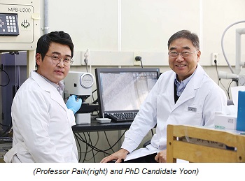
A research team under Professor Kyung-Wook Paik in the Department of Materials developed an anchoring polymer layer structure that can effectively suppress the movement of conductive particles during the bonding process of the anisotropic conductive films (ACFs). The new structure will significantly improve the conductive particle capture rate, addressing electrical short problems in the ultra-fine pitch assembly process.
During the ultra-fine pitch bonding process, the conductive particles of conventional ACFs agglomerate between bumps and cause electrical short circuits. To overcome the electrical shortage problem caused by the free movement of conductive particles, higher tensile strength anchoring polymer layers incorporated with conductive particles were introduced into the ACFs to effectively prevent conductive particle movement.
The team used nylon to produce a single layer film with well-distributed and incorporated conductive particles. The higher tensile strength of nylon completely suppressed the movement of conductive particles, raising the capture rate of conductive particles from 33% of the conventional ACFs to 90%. The nylon films showed no short circuit problem during the Chip on Glass assembly. Even more, they obtained excellent electrical conductivity, high reliability, and low cost ACFs during the ultra-fine pitch applications.
Professor Paik believes this new type of ACFs can further be applied not only to VR, 4K and 8K UHD display products, but also to large-size OLED panels and mobile devices.
His team completed a prototype of the film supported by the ‘H&S High-Tech,’ a domestic company and the ‘Innopolis Foundation.’ The study, whose first author is PhD candidate Dal-Jin Yoon, is described in the October issue of IEEE TCPMT.
Figure 1: Schematic process of APL structure fabrication.
Figure 2: Prototype production of APL ACFs.
Share on:


Suggested Items
Electrolube Launch Range of Silver Conductive Inks for LCD, LCM and OLED Display Applications at C-Touch & Display China
11/22/2023 | ElectrolubeElectrolube, global manufacturer of specialist electro-chemical solutions, has announced the launch of a brand-new series of silver conductive inks for multiple adhesive processes designed for use during the manufacture of LCD, LCM, and OLED displays and display modules for mobile/smart phones, tablets and many other electronic products.
Meta Materials, Panasonic Industry Collaborate on Next Generation Transparent Conductive Materials
10/02/2023 | ACN NewswireThis joint effort is expected to strengthen the supply of NANOWEB® films and accelerate the growth of the transparent conductive film industry, offering new applications for the automotive and consumer electronics sectors, such as transparent film antennas, transparent film heaters, and transparent film electromagnetic shielding.
IDTechEx Explores How EMI Shielding is Enabling Compact Electronics
09/26/2023 | PRNewswireIt is no secret that electronic devices are becoming increasingly compact, with greater functionality contained in smaller volumes.
Trouble in Your Tank: Processes to Support IC Substrates and Advanced Packaging, Part 4
09/28/2023 | Michael Carano -- Column: Trouble in Your TankIn a previous column, the critical process of desmear and its necessity to ensure a clean copper surface connection was presented. Now, my discussion will focus on obtaining a void-free and tightly adherent copper plating deposit on these surfaces. After the desmear process, the task is to insure a continuous, conductive, and void-free deposit on the via walls and capture pad. Today, there are several processes that can be utilized to render vias conductive.
IDTechEx Asks Where Flexible Hybrid Electronics Add the Most Value
09/11/2023 | PRNewswireCan digital and/or high throughput manufacturing be applied to circuit boards? Can stretchable electronics be produced without sacrificing processing capabilities?