


 The Right Approach: I Hear the Train A Comin'
 It’s Only Common Sense: OCCAM—the Time Is Now
 Marcy's Musings: The Growing Industry
Solution for Next Generation Nanochips Comes Out of Thin Air
November 20, 2018 | RMIT UniversityEstimated reading time: 2 minutes
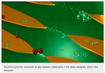
Researchers at RMIT University have engineered a new type of transistor, the building block for all electronics. Instead of sending electrical currents through silicon, these transistors send electrons through narrow air gaps, where they can travel unimpeded as if in space.
The device unveiled in material sciences journal Nano Letters, eliminates the use of any semiconductor at all, making it faster and less prone to heating up.
Lead author and PhD candidate in RMIT’s Functional Materials and Microsystems Research Group, Ms Shruti Nirantar, said this promising proof-of-concept design for nanochips as a combination of metal and air gaps could revolutionise electronics. “Every computer and phone has millions to billions of electronic transistors made from silicon, but this technology is reaching its physical limits where the silicon atoms get in the way of the current flow, limiting speed and causing heat,” Nirantar said.
“Our air channel transistor technology has the current flowing through air, so there are no collisions to slow it down and no resistance in the material to produce heat.”
Moore's Law
The power of computer chips—or number of transistors squeezed onto a silicon chip—has increased on a predictable path for decades, roughly doubling every two years. But this rate of progress, known as Moore’s Law, has slowed in recent years as engineers struggle to make transistor parts, which are already smaller than the tiniest viruses, smaller still.
Nirantar says their research is a promising way forward for nano electronics in response to the limitation of silicon-based electronics. “This technology simply takes a different pathway to the miniaturisation of a transistor in an effort to uphold Moore’s Law for several more decades,” Shruti said.
A New Way Forward
Research team leader Associate Professor Sharath Sriram said the design solved a major flaw in traditional solid channel transistors—they are packed with atoms—which meant electrons passing through them collided, slowed down and wasted energy as heat.
“Imagine walking on a densely crowded street in an effort to get from point A to B. The crowd slows your progress and drains your energy,” Sriram said. “Travelling in a vacuum on the other hand is like an empty highway where you can drive faster with higher energy efficiency.”
But while this concept is obvious, vacuum packaging solutions around transistors to make them faster would also make them much bigger, so are not viable.
“We address this by creating a nanoscale gap between two metal points. The gap is only a few tens of nanometers, or 50,000 times smaller than the width of a human hair, but it’s enough to fool electrons into thinking that they are travelling through a vacuum and re-create a virtual outer-space for electrons within the nanoscale air gap,” he said.
The nanoscale device is designed to be compatible with modern industry fabrication and development processes. It also has applications in space—both as electronics resistant to radiation and to use electron emission for steering and positioning ‘nano-satellites.’
“This is a step towards an exciting technology which aims to create something out of nothing to significantly increase speed of electronics and maintain pace of rapid technological progress,” Sriram said.
This work was undertaken at RMIT University’s cutting-edge Micro Nano Research Facility and with support of the Victorian node of the Australian National Fabrication Facility.
Story: Michael Quin
Share on:


Suggested Items
Book Excerpt: The Printed Circuit Assembler’s Guide to... Factory Analytics
04/24/2024 | I-Connect007 Editorial TeamIn our fast-changing, deeply competitive, and margin-tight industry, factory analytics can be the key to unlocking untapped improvements to guarantee a thriving business. On top of that, electronics manufacturers are facing a tremendous burden to do more with less. If you don't already have a copy of this book, what follows is an excerpt from the introduction chapter of 'The Printed Circuit Assembler’s Guide to... Factory Analytics: Unlocking Efficiency Through Data Insights' to whet your appetite.
Listen Up! The Intricacies of PCB Drilling Detailed in New Podcast Episode
04/25/2024 | I-Connect007In episode 5 of the podcast series, On the Line With: Designing for Reality, Nolan Johnson and Matt Stevenson continue down the manufacturing process, this time focusing on the post-lamination drilling process for PCBs. Matt and Nolan delve into the intricacies of the PCB drilling process, highlighting the importance of hole quality, drill parameters, and design optimization to ensure smooth manufacturing. The conversation covers topics such as drill bit sizes, aspect ratios, vias, challenges in drilling, and ways to enhance efficiency in the drilling department.
Elevating PCB Design Engineering With IPC Programs
04/24/2024 | Cory Blaylock, IPCIn a monumental stride for the electronics manufacturing industry, IPC has successfully championed the recognition of the PCB Design Engineer as an official occupation by the U.S. Department of Labor (DOL). This pivotal achievement not only underscores the critical role of PCB design engineers within the technology landscape, but also marks the beginning of a transformative journey toward nurturing a robust, skilled workforce ready to propel our industry into the future.
Winner of The Science Show Rakett 69 Receives Incap Scholarship
04/24/2024 | IncapThe winner of the Rakett 69 science show, Andri Türkson, who stood out as an electronics enthusiast, received a scholarship from Incap Estonia, along with an internship opportunity in Saaremaa.
Alternative Manufacturing Inc. Awarded QML Requalification to IPC J-STD-001 and IPC-A-610
04/24/2024 | IPCIPC's Validation Services Program has awarded an IPC J-STD-001 and IPC-A-610 Qualified Manufacturers Listing (QML) requalification to Alternative Manufacturing Inc (AMI).