


 The Right Approach: I Hear the Train A Comin'
 It’s Only Common Sense: OCCAM—the Time Is Now
 Marcy's Musings: The Growing Industry
New Graphene-based Sensor Design Could Improve Food Safety
December 5, 2018 | The Optical SocietyEstimated reading time: 2 minutes
In the U.S., more than 100 food recalls were issued in 2017 because of contamination from harmful bacteria such as Listeria, Salmonella or E. coli. A new sensor design could one day make it easier to detect pathogens in food before products hit the supermarket shelves, thus preventing sometimes-deadly illnesses from contaminated food.
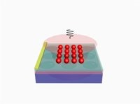
Image Caption: Researchers designed a new sensor with an array of nanoscale graphene disks that each contain an off-center hole. When light from above hits the arrays, the interaction between the disks and their holes increases the sensitivity of the sensor and enables the detection of two substances at once (red balls). The disks are located between an ion-gel (green) and calcium fluoride (dark pink) layers, which are used to apply a voltage to the sensor and to aid in the generation of a surface plasmon, respectively.
In the journal Optical Materials Express, researchers report a new design for a sensor that can simultaneously detect multiple substances including dangerous bacteria and other pathogens. In addition to food safety, the new design could improve detection of gases and chemicals for a wide range of other applications.
“Our design is based on graphene sheets, which are two-dimensional crystals of carbon just one atom thick,” said research team member Bing-Gang Xiao, from China Jiliang University. “The sensor is not only highly sensitive but can also be easily adjusted to detect different substances.”
Sensing with Graphene
The excellent optical and electronic properties of graphene make it attractive for sensors that use electromagnetic waves known as plasmons that propagate along the surface of a conducting material in response to light exposure. A substance can be detected by measuring how the refractive index of the sensor changes when a substance of interest is close to the graphene’s surface.
Researchers have taken advantage of graphene’s unique properties to create sensors and materials for a range of applications in recent years. Compared to metals like gold and silver, graphene exhibits stronger plasmon waves with longer propagation distances. In addition, the wavelength at which graphene is responsive can be changed by applying a polarization voltage instead of recreating the whole device. However, few previous research efforts have demonstrated sensitive graphene sensors that work with the infrared wavelengths necessary to detect bacteria and biomolecules.
For the new sensor, the researchers used theoretical calculations and simulations to design an array of nanoscale graphene disks that each contain an off-center hole. The sensor includes ion-gel and silicon layers that can be used to apply a voltage to tune the graphene’s properties for detection of various substances.
The interaction between the disks and their holes creates what is known as the plasmon hybridization effect, which increases the sensitivity of the device. The hole and the disk also create different wavelength peaks that can each be used to detect the presence of different substances simultaneously.
Simulations performed by the researchers using mid-infrared wavelengths showed that their new sensor platform would be more sensitive to substances present in gases, liquids or solids than using discs without holes.
The researchers are now working to improve the process that would be used to make the array of nanoscale discs. The accuracy at which these structures are fabricated will greatly impact the performance of the sensor.
“We also want to explore whether the graphene plasmon hybridization effect could be used to aid the design of dual-band mid-infrared optical communication devices,” said Xiao.
Share on:


Suggested Items
iNEMI Packaging Tech Topic Series: Role of EDA in Advanced Semiconductor Packaging
04/26/2024 | iNEMIAdvanced semiconductor packaging with heterogenous integration has made on-package integration of multiple chips a crucial part of finding alternatives to transistor scaling. Historically, EDA tools for front-end and back-end design have evolved separately; however, design complexity and the increased number of die-to-die or die-to-substrate interconnections has led to the need for EDA tools that can support integration of overall design planning, implementation, and system analysis in a single cockpit.
Cadence, TSMC Collaborate on Wide-Ranging Innovations to Transform System and Semiconductor Design
04/25/2024 | Cadence Design SystemsCadence Design Systems, Inc. and TSMC have extended their longstanding collaboration by announcing a broad range of innovative technology advancements to accelerate design, including developments ranging from 3D-IC and advanced process nodes to design IP and photonics.
Ansys, TSMC Enable a Multiphysics Platform for Optics and Photonics, Addressing Needs of AI, HPC Silicon Systems
04/25/2024 | PRNewswireAnsys announced a collaboration with TSMC on multiphysics software for TSMC's Compact Universal Photonic Engines (COUPE). COUPE is a cutting-edge Silicon Photonics (SiPh) integration system and Co-Packaged Optics platform that mitigates coupling loss while significantly accelerating chip-to-chip and machine-to-machine communication.
Siemens’ Breakthrough Veloce CS Transforms Emulation and Prototyping with Three Novel Products
04/24/2024 | Siemens Digital Industries SoftwareSiemens Digital Industries Software launched the Veloce™ CS hardware-assisted verification and validation system. In a first for the EDA (Electronic Design Automation) industry, Veloce CS incorporates hardware emulation, enterprise prototyping and software prototyping and is built on two highly advanced integrated circuits (ICs) – Siemens’ new, purpose-built Crystal accelerator chip for emulation and the AMD Versal™ Premium VP1902 FPGA adaptive SoC (System-on-a-chip) for enterprise and software prototyping.
Listen Up! The Intricacies of PCB Drilling Detailed in New Podcast Episode
04/25/2024 | I-Connect007In episode 5 of the podcast series, On the Line With: Designing for Reality, Nolan Johnson and Matt Stevenson continue down the manufacturing process, this time focusing on the post-lamination drilling process for PCBs. Matt and Nolan delve into the intricacies of the PCB drilling process, highlighting the importance of hole quality, drill parameters, and design optimization to ensure smooth manufacturing. The conversation covers topics such as drill bit sizes, aspect ratios, vias, challenges in drilling, and ways to enhance efficiency in the drilling department.