


 Marcy's Musings: The Growing Industry
 It’s Only Common Sense: Here’s What To Do After IPC APEX EXPO 2024
 Dan’s Biz Bookshelf: Seeing the How
A 3D Imaging Technique Unlocks Properties of Perovskite Crystals
December 6, 2018 | Pennsylvania State UniversityEstimated reading time: 4 minutes
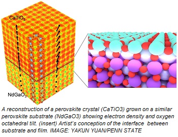
A team of materials scientists from Penn State, Cornell and Argonne National Laboratory have, for the first time, visualized the 3D atomic and electron density structure of the most complex perovskite crystal structure system decoded to date.
Perovskites are minerals that are of interest as electrical insulators, semiconductors, metals or superconductors, depending on the arrangement of their atoms and electrons.
Perovskite crystals have an unusual grouping of oxygen atoms that form an octahedron — an eight-sided polygon. This arrangement of oxygen atoms acts like a cage that can hold a large number of the elemental atoms in the periodic table. Additionally, other atoms can be fixed to the corners of a cube outside of the cage at precise locations to alter the material’s properties, for instance in changing a metal into an insulator, or a non-magnet into a ferromagnet.
In their current work, the team grew the very first discovered perovskite crystal, called calcium titanate, on top of a series of other perovskite crystal substrates with similar but slightly different oxygen cages at their surfaces. Because the thin film perovskite on top wants to conform to the structure of the thicker substrate, it contorts its cages in a process known as tilt epitaxy. The researchers found this tilt epitaxy of calcium titanate caused a very ordinary material to become ferroelectric — a spontaneous polarization — and to remain ferroelectric up to 900 Kelvin, around three times hotter than room temperature. They were also able to visualize the three-dimensional electron density distribution in calcium titanate thin film for the first time.
“We have been able to see atoms for quite some time, but not map them and their electron distribution in space in a crystal in three dimensions,” said Venkat Gopalan, professor of materials science and physics, Penn State. “If we can see not just where atomic nuclei are located in space, but also how their electron clouds are shared, that will tell us basically everything we need to know about the material in order to infer its properties.”
That was the challenge the team set for itself over five years ago when Gopalan gave the project to his student and lead author of a new report in Nature Communications, Yakun Yuan,. Based on a rarely used x-ray visualization technique called COBRA, (coherent Bragg rod analysis) originally developed by a group in Israel, Yuan figured out how to expand and modify the technique to analyze one of the most complicated, least symmetrical material systems studied to date. This system is a strained three-dimensional perovskite crystal with octahedral tilts in all directions, grown on another equally complex crystal structure.
“To reveal 3D structural details at the atomic level, we had to collect extensive datasets using the most brilliant synchrotron X-ray source available at Argonne National Labs and carefully analyze them with the COBRA analysis code modified for accommodating the complexity of such low symmetry,” said Yuan.
Gopalan went on to explain that very few perovskite oxygen cages are perfectly aligned throughout the material. Some rotate counterclockwise in one layer of atoms and clockwise in the next. Some cages are squeezed out of shape or tilt in directions that are in or out of plane to the substrate surface. From the interface of a film with the substrate it is grown on, all the way to its surface, each atomic layer may have unique changes in their structure and pattern. All of these distortions make a difference in the material properties, which they can predict using a computational technique called density functional theory (DFT).
“The predictions from the DFT calculations provide insights that complement the experimental data and help explain the way that material properties change with the alignment or tilting of the perovskite oxygen cages,” said Susan Sinnott, head and professor of Materials Science and Engineering, whose group performed the theoretical calculations.
The team also validated their advanced COBRA technique against multiple images of their material using the powerful Titan transmission electron microscope in the Materials Research Institute at Penn State. Since the electron microscopes image extremely thin electron transparent samples in a 2D projection, not all of the 3D image could be captured even with the best microscope available today and with multiple sample orientations. This is an area where 3D dimensional imaging by the COBRA technique outperformed the electron microscopy in such complex structures.
The researchers believe their COBRA technique is applicable to the study of many other 3D, low-symmetry atomic crystals.
Additional authors on “Three-dimensional atomic scale electron density reconstruction of octahedral tilt epitaxy in functional perovskites” Yanfu Lu, a Ph.D. student in Sinnott’s group, Greg Stone, Gopalan’s former postdoctoral scholar, Ke Wang, a staff scientist in Penn State’s Materials Research Institute, Darrell Schlom and his Ph.D. student Charles Brooks, Cornell University, and Hua Zhou, staff scientist, Argonne National Laboratory.
The National Science Foundation funded this project with additional support provided through the Department of Energy and the Penn State 2D Crystal Consortium, a NSF Materials Innovation Platform, and the Penn State institute for CyberScience.
Share on:


Suggested Items
Groundbreaking Ceremony Marks the Beginning of a New Era for Newccess Industrial; The Construction of the MINGXIN Building
04/12/2024 | Newccess IndustrialOn a clear and sunny day in March, the groundbreaking ceremony for the MINGXIN Building took place in Shenzhen, China. This moment marked the official commencement of construction for a project that will reshape the semiconductor materials industry.
The Need for a Holistic Global Sustainability Standard
04/10/2024 | Michael Ford, Aegis SoftwareNo one can deny that the resources of our fragile planet are finite. The environment seems like a third party, subject to constant degradation. We’re acutely aware of the effects of pollution on our climate, and despite our “throw-away” culture, recycling and recovery of materials has remained relatively expensive, even as we use more energy just to survive.
iNEMI Publishes Four Roadmap Topics
04/04/2024 | iNEMIThe International Electronics Manufacturing Initiative (iNEMI) announces the availability of the first roadmap topics in the new iNEMI Roadmap format. Printed circuit boards, sustainable electronics, smart manufacturing, and mmWave materials and test are now available online.
Insulectro’s 'Storekeepers' Extend Their Welcome to Technology Village at IPC APEX EXPO
04/03/2024 | InsulectroInsulectro, the largest distributor of materials for use in the manufacture of PCBs and printed electronics, welcomes attendees to its TECHNOLOGY VILLAGE during this year’s IPC APEX EXPO at the Anaheim Convention Center, April 9-11, 2024.
Checking In With ICAPE Group
04/03/2024 | Nolan Johnson, I-Connect007ICAPE Group’s field application engineer Erik Pederson drills down on sustainability, supply chain resiliency, and what value engineering really looks like in this exclusive interview. Founded in 1999, European-based ICAPE Group provides 21 million printed circuit boards and over six million technical parts to manufacturers every month. With 30 PCB manufacturing partners globally and 50 partners providing a wide array of technical parts, ICAPE Group has operations in China, Taiwan, Thailand, South Korea, Vietnam, South Africa, Europe, Mexico, and the United States. The company also focuses on the value proposition for its customers.