


 Marcy's Musings: The Growing Industry
 It’s Only Common Sense: Here’s What To Do After IPC APEX EXPO 2024
 Dan’s Biz Bookshelf: Seeing the How
Form-Fitting, Nanoscale Sensors Now Make Sense
December 6, 2018 | Rice UniversityEstimated reading time: 3 minutes
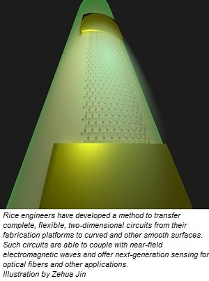
What if a sensor sensing a thing could be part of the thing itself? Rice University engineers believe they have a two-dimensional solution to do just that.
Rice engineers led by materials scientists Pulickel Ajayan and Jun Lou have developed a method to make atom-flat sensors that seamlessly integrate with devices to report on what they perceive.
Electronically active 2D materials have been the subject of much research since the introduction of graphene in 2004. Even though they are often touted for their strength, they’re difficult to move to where they’re needed without destroying them.
The Ajayan and Lou groups, along with the lab of Rice engineer Jacob Robinson, have a new way to keep the materials and their associated circuitry, including electrodes, intact as they’re moved to curved or other smooth surfaces.
The Rice team tested the concept by making a 10-nanometer-thick indium selenide photodetector with gold electrodes and placing it onto an optical fiber. Because it was so close, the near-field sensor effectively coupled with an evanescent field – the oscillating electromagnetic wave that rides the surface of the fiber—and accurately detected the flow of information inside.
The benefit is that these sensors can now be imbedded into such fibers where they can monitor performance without adding weight or hindering the signal flow.
“This paper proposes several interesting possibilities for applying 2D devices in real applications,” Lou said. “For example, optical fibers at the bottom of the ocean are thousands of miles long, and if there’s a problem, it’s hard to know where it occurred. If you have these sensors at different locations, you can sense the damage to the fiber.”
Lou said labs have gotten good at transferring the growing roster of 2D materials from one surface to another, but the addition of electrodes and other components complicates the process. “Think about a transistor,” he said. “It has source, drain and gate electrodes and a dielectric (insulator) on top, and all of these have to be transferred intact. That’s a very big challenge, because all of those materials are different.”
Raw 2D materials are often moved with a layer of polymethyl methacrylate (PMMA), more commonly known as Plexiglas, on top, and the Rice researchers make use of that technique. But they needed a robust bottom layer that would not only keep the circuit intact during the move but could also be removed before attaching the device to its target. (The PMMA is also removed when the circuit reaches its destination.)
The ideal solution was polydimethylglutarimide (PMGI), which can be used as a device fabrication platform and easily etched away before transfer to the target. “We’ve spent quite some time to develop this sacrificial layer,” Lou said. PMGI appears to work for any 2D material, as the researchers experimented successfully with molybdenum diselenide and other materials as well.
The Rice labs have only developed passive sensors so far, but the researchers believe their technique will make active sensors or devices possible for telecommunication, biosensing, plasmonics and other applications.
Rice graduate student Zehua Jin is lead author of the paper. Co-authors are Rice graduate students Fan Ye, Shuai Jia and Liangliang Dong and postdoctoral researcher Xiang Zhang; Rice alumnus Sidong Lei, now an assistant professor at Georgia State University, and Robert Vajtai, a research professor in materials science and nanoengineering at Rice. Ajayan is chair of Rice’s Department of Materials Science and NanoEngineering, the Benjamin M. and Mary Greenwood Anderson Professor in Engineering and a professor of chemistry. Lou is a professor of materials science and nanoengineering. Robinson is an assistant professor of electrical and computer engineering.
The research was supported by the Air Force Office of Scientific Research, the Welch Foundation, Rice IDEA and Function Accelerate nanoMaterial Engineering (FAME), one of six centers of the Semiconductor Technology Advanced Research Network sponsored by the Microelectronics Advanced Research Corporation and the Defense Advanced Research Projects Agency.
Share on:


Suggested Items
Groundbreaking Ceremony Marks the Beginning of a New Era for Newccess Industrial; The Construction of the MINGXIN Building
04/12/2024 | Newccess IndustrialOn a clear and sunny day in March, the groundbreaking ceremony for the MINGXIN Building took place in Shenzhen, China. This moment marked the official commencement of construction for a project that will reshape the semiconductor materials industry.
The Need for a Holistic Global Sustainability Standard
04/10/2024 | Michael Ford, Aegis SoftwareNo one can deny that the resources of our fragile planet are finite. The environment seems like a third party, subject to constant degradation. We’re acutely aware of the effects of pollution on our climate, and despite our “throw-away” culture, recycling and recovery of materials has remained relatively expensive, even as we use more energy just to survive.
iNEMI Publishes Four Roadmap Topics
04/04/2024 | iNEMIThe International Electronics Manufacturing Initiative (iNEMI) announces the availability of the first roadmap topics in the new iNEMI Roadmap format. Printed circuit boards, sustainable electronics, smart manufacturing, and mmWave materials and test are now available online.
Insulectro’s 'Storekeepers' Extend Their Welcome to Technology Village at IPC APEX EXPO
04/03/2024 | InsulectroInsulectro, the largest distributor of materials for use in the manufacture of PCBs and printed electronics, welcomes attendees to its TECHNOLOGY VILLAGE during this year’s IPC APEX EXPO at the Anaheim Convention Center, April 9-11, 2024.
Checking In With ICAPE Group
04/03/2024 | Nolan Johnson, I-Connect007ICAPE Group’s field application engineer Erik Pederson drills down on sustainability, supply chain resiliency, and what value engineering really looks like in this exclusive interview. Founded in 1999, European-based ICAPE Group provides 21 million printed circuit boards and over six million technical parts to manufacturers every month. With 30 PCB manufacturing partners globally and 50 partners providing a wide array of technical parts, ICAPE Group has operations in China, Taiwan, Thailand, South Korea, Vietnam, South Africa, Europe, Mexico, and the United States. The company also focuses on the value proposition for its customers.