


 The Right Approach: I Hear the Train A Comin'
 It’s Only Common Sense: OCCAM—the Time Is Now
 Marcy's Musings: The Growing Industry
Cutting and Pasting with Graphene
December 12, 2018 | University of LeidenEstimated reading time: 2 minutes
To date it has proved very difficult to convert the promises of the miracle material graphene into practical applications. Amedeo Bellunato, PhD candidate at the Leiden Institute of Chemistry, has developed a method of cutting graphene into smaller fragments using a diamond knife. He can then construct nanostructures from the fragments.
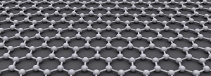
Graphene is a honeycomb structure of carbon atoms just a single atom thick. After its discovery in 2004, it seemed to be the ideal basic material for nanotechnology applications: it is super strong and it is an exceptionally good conductor of both heat and electricity. In 2013 the EU launched theGraphene Flagship a research programme with a budget of a billion euros to develop such applications as more efficient solar cells, LEDs, batteries and all kinds of sensors.
However, in his dissertation, Bellunato states that making such nanostructures is still an extremely complex production process that does not lend itself well to serial production. Also, it has proven almost impossible to selectively 'functionalize' graphene chemically, i.e. to connect other chemical elements, such as oxygen or nitrogen atoms, to the edges of a graphene nanostructure. It is important to be able to do this in order to make graphene into a versatile nanomaterial with multiple applications.
The microtome that cuts exceptionally precise strips of of graphene. The sandwich with the graphene (inset) is the transparent block to the left, the diamond knife can be seen at the edge of the blue container.
Graphene Sandwich
Inspired by earlier experiments, Bellunato decided to take a different approach, namely to take a sandwich of plastic and metal with a layer of graphene in the middle, and to literally cut it into fragments. He does this using a microtome, a diamond knife that can cut fragments with nanometre precision.
In the cutting edge of the sandwich, a perfectly clean, one-atom-thick edge of graphene is exposed, to which other atoms or molecules can be connected by chemical means. The graphene slice can also be connected to an electrical current, turning it into an electrochemical cell. This can be compared with the electrochemical coating of a metal, but then at nanoscale, since only the edge of the graphene is coated. Bellunato was also able to build a sandwich of nanopores and nanogaps of graphene using microscopically thin strips.
Kruiselings
It also proved possible to make a so-called tunnel junction. This occurs between two electrical conductors, when they are within a few nanometres of one another at a particular point. A minuscule current can then flow between the two conductors. As the flow of energy is very sensitive to the distance between the conductors, this tunnel effect forms the basis for all kinds of extremely sensitive sensors.
Bellunato: 'This tunnel junction is not new. It is a matter of refining the technique, and then it should have practical applications within five years or so.' The unconventional technique that he developed will not primarily be used in consumer products, he expects, but rather in advanced research instruments.
Text: Arnout Jaspers
Share on:


Suggested Items
indie Semiconductor Launches Advanced Smart Connectivity Solutions for In-Cabin Applications
04/23/2024 | indie Semiconductorindie Semiconductor, Inc., an Autotech solutions innovator, has introduced a family of new high-performance video converters and retimers to enable in-cabin connectivity applications, including audio and video transport and device interfacing.
IDTechEx Discusses the Role of Printed Sensors in Mass-Digitization
04/11/2024 | PRNewswireIntegrated sensors digitizing physical interactions are vital in everyday life. From personalized user experiences to warehouse inventory management, data-driven insights are driving demand for smarter sensors — and lots of them.
MKS Introduces ESI Geode G2 CO2 Laser System for High- Precision and High-Speed HDI and mSap Via Drilling
04/09/2024 | MKS Instruments, Inc.MKS Instruments, Inc., a global provider of technologies that transform our world, today announced the official launch of the ESI Geode™ G2 laser drill system, the next generation of the Geode™ platform for processing PCB and ICP materials.
DuPont Unveils Pyralux ML Laminate Series, Offering High Thermal Management for Extreme Environments
04/09/2024 | DuPontDuPont introduced the DuPont™ Pyralux® ML Series of double-sided metal-clad laminates, a unique addition to its extensive family of Pyralux® laminates for flexible and rigid-flex printed circuit boards (PCBs).
A Closer Look at Professional Development at IPC APEX EXPO 2024: 3D Printing and AI
04/09/2024 | I-Connect007 Editorial TeamWhile the finishing touches were being made to the show floor at IPC APEX EXPO, just as much activity was happening in the conference rooms of the Anaheim Convention Center on the days before the show officially opened. The hallways and classrooms were filled for standards committee development meetings and Professional Development Courses, and IPC hosted evening receptions for Emerging Engineers, ECWC, and those who are attending for the first time in a special “newcomers” event.