


 The Right Approach: I Hear the Train A Comin'
 It’s Only Common Sense: OCCAM—the Time Is Now
 Marcy's Musings: The Growing Industry
Scientists Design New Material to Harness Power of Light
December 18, 2018 | UMass LowellEstimated reading time: 2 minutes
Scientists have long known that synthetic materials—called metamaterials—can manipulate electromagnetic waves such as visible light to make them behave in ways that cannot be found in nature. That has led to breakthroughs such as super-high resolution imaging. Now, UMass Lowell is part of a research team that is taking the technology of manipulating light in a new direction.
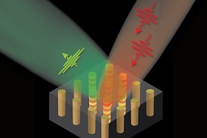
Image Caption: This illustration shows two incoming (red) photons being converted into one reflected (green) photon as result of light interaction with the nanowire structure in the metamaterial. The nanowires are about 100 nanometers apart from center to center, which is about one-fifty-thousandth the diameter of human hair.
The team—which includes collaborators from UMass Lowell, King’s College London, Paris Diderot University and the University of Hartford—has created a new class of metamaterial that can be “tuned” to change the color of light. This technology could someday enable on-chip optical communication in computer processors, leading to smaller, faster, cheaper and more power-efficient computer chips with wider bandwidth and better data storage, among other improvements. On-chip optical communication can also create more efficient fiber-optic telecommunication networks.
“Today’s computer chips use electrons for computing. Electrons are good because they’re tiny,” said Prof. Viktor Podolskiy of the Department of Physics and Applied Physics, who is the project’s principal investigator at UMass Lowell. “However, the frequency of electrons is not fast enough. Light is a combination of tiny particles, called photons, which don’t have mass. As a result, photons could potentially increase the chip’s processing speed.”
By converting electrical signals into pulses of light, on-chip communication will replace obsolete copper wires found on conventional silicon chips, Podolskiy explained. This will enable chip-to-chip optical communication and, ultimately, core-to-core communication on the same chip.
“The end result would be the removal of the communication bottleneck, making parallel computing go so much faster,” he said, adding that the energy of photons determines the color of light. “The vast majority of everyday objects, including mirrors, lenses and optical fibers, can steer or absorb these photons. However, some materials can combine several photons together, resulting in a new photon of higher energy and of different color.”
Podolskiy says enabling the interaction of photons is key to information processing and optical computing. “Unfortunately, this nonlinear process is extremely inefficient and suitable materials for promoting the photon interaction are very rare.”
Podolskiy and the research team have discovered that several materials with poor nonlinear characteristics can be combined together, resulting in a new metamaterial that exhibits desired state-of-the-art nonlinear properties.
“The enhancement comes from the way the metamaterial reshapes the flow of photons,” he said. “The work opens a new direction in controlling the nonlinear response of materials and may find applications in on-chip optical circuits, drastically improving on-chip communications.”
Share on:


Suggested Items
Designer’s Notebook: What Designers Need to Know About Manufacturing, Part 2
04/24/2024 | Vern Solberg -- Column: Designer's NotebookThe printed circuit board (PCB) is the primary base element for providing the interconnect platform for mounting and electrically joining electronic components. When assessing PCB design complexity, first consider the component area and board area ratio. If the surface area for the component interface is restricted, it may justify adopting multilayer or multilayer sequential buildup (SBU) PCB fabrication to enable a more efficient sub-surface circuit interconnect.
Insulectro’s 'Storekeepers' Extend Their Welcome to Technology Village at IPC APEX EXPO
04/03/2024 | InsulectroInsulectro, the largest distributor of materials for use in the manufacture of PCBs and printed electronics, welcomes attendees to its TECHNOLOGY VILLAGE during this year’s IPC APEX EXPO at the Anaheim Convention Center, April 9-11, 2024.
ENNOVI Introduces a New Flexible Circuit Production Process for Low Voltage Connectivity in EV Battery Cell Contacting Systems
04/03/2024 | PRNewswireENNOVI, a mobility electrification solutions partner, introduces a more advanced and sustainable way of producing flexible circuits for low voltage signals in electric vehicle (EV) battery cell contacting systems.
Heavy Copper PCBs: Bridging the Gap Between Design and Fabrication, Part 1
04/01/2024 | Yash Sutariya, Saturn Electronics ServicesThey call me Sparky. This is due to my talent for getting shocked by a variety of voltages and because I cannot seem to keep my hands out of power control cabinets. While I do not have the time to throw the knife switch to the off position, that doesn’t stop me from sticking screwdrivers into the fuse boxes. In all honesty, I’m lucky to be alive. Fortunately, I also have a talent for building high-voltage heavy copper circuit boards. Since this is where I spend most of my time, I can guide you through some potential design for manufacturability (DFM) hazards you may encounter with heavy copper design.
Trouble in Your Tank: Supporting IC Substrates and Advanced Packaging, Part 5
03/19/2024 | Michael Carano -- Column: Trouble in Your TankDirect metallization systems based on conductive graphite or carbon dispersion are quickly gaining acceptance worldwide. Indeed, the environmental and productivity gains one can achieve with these processes are outstanding. In today’s highly competitive and litigious environment, direct metallization reduces costs associated with compliance, waste treatment, and legal issues related to chemical exposure. What makes these processes leaders in the direct metallization space?