


 Marcy's Musings: The Growing Industry
 It’s Only Common Sense: Here’s What To Do After IPC APEX EXPO 2024
 Dan’s Biz Bookshelf: Seeing the How
Better Characterization of Ultra-Thin Materials
December 27, 2018 | DTUEstimated reading time: 3 minutes
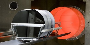
A new optical technology may revolutionize the semiconductor industry and create brand new possibilities within sustainable electronics and data handling. The project is subsidized by Innovation Fund Denmark.
We take it for granted that a new smartphone or tablet is faster than its obsolete predecessor. It has more memory, is thinner, and its touch screen is crystal-clear with a fast response rate. In a few years it may even be flexible, allowing you to roll it up and put it in your pocket.
We expect that renewable energy from solar and wind power will become increasingly efficient and profitable, and that electric cars and trains will play a major role in a future sustainable society and for our environment.
The semiconductor industry is one of the driving forces behind this development. It provides the processing power for handling the astronomical data volumes produced, and delivers efficient components for high-power electronics.
The new Innovation Fund project TRIM has a total budget of EUR 3.7 million (DKK 27 million) and is subsidized by Innovation Fund Denmark with EUR 2.6 million (DKK 19 million).
The aim is to develop optical technology based on terahertz radiation, which can measure the quality of electric and magnetic materials for the semiconductor industry. This ensures high-quality and homogeneous materials.
“Some of the key words for the continued development of a sustainable information society is increased speed, greater storage capacity and higher reliability. All of these require control and quality assurance. Terahertz technology has been the focus of research around the world for many years—now the time has come to bring a huge basic research investment into the real world and prove the value of the technology,” says Peter Uhd Jepsen, Professor, DTU Fotonik, who will be heading the project for the next three years.
The technology offers unique opportunities for completely contactless measurements—a property in high demand by industry, and an essential requirement for the characterization of e.g. 2D materials consisting of one or only a few layers of atoms.
The development of the TRIM technology takes place in close collaboration between DTU and the companies Capres A/S, Topsil GlobalWafers A/S, and NKT Photonics A/S.
The project links the world’s leading competences within terahertz and laser technology, silicon fabrication, and semiconductor materials characterization. It introduces completely new technology and methodology into a conservative and notoriously cautious industry.
“Denmark has a strong position within characterization of materials for the semiconductor industry, but there is still some way to go before we can roll out our laboratory experience to industry. The investment from Innovation Fund Denmark will help us overcome the technological and commercial barriers, which are completely natural, but must be broken down to ensure acceptance of new technologies and methods,” says Peter Uhd Jepsen.
Three of Denmark’s leading companies within semiconductors participate in the project and see great opportunities in getting direct access to world-leading research within this area:
“Capres A/S expects the TRIM project to lead to a significant expansion of the market potential for sales of advanced and fully automated machines to both current and new semiconductor industry customers. For Capres A/S, this will entail that the current unique multi-pin nanoprobe and microprobe-based measuring technique, combined with the new contactless optical measurements, extends the scope and measuring speed within materials characterization, process optimization, and process control,” says Peter Folmer Nielsen, CTO and co-founder, Capres A/S.
“NKT Photonics A/S has achieved great success since its founding by being at the forefront where technology is created. The TRIM project is a prime example of a technology under development with the potential to strengthen Danish high-tech industry as a key supplier to the huge semiconductor industry. The role of NKT Photonics A/S in TRIM is to develop and supply laser systems for the project. The project has extremely high phase noise requirements for the laser systems
Share on:


Suggested Items
Three Industry Leaders Receive IPC President’s Award
04/17/2024 | IPCIn recognition of their leadership and significant contributions of time and talent to IPC and the electronics industry, three IPC volunteers were presented with the IPC President’s Award at IPC APEX EXPO in Anaheim, Calif., on April 9, 2024.
Real Time with... IPC APEX EXPO 2024: IPC Government Relations Holds Lawmakers Accountable
04/16/2024 | Real Time with...IPC APEX EXPOThe IPC Government Relations team is constantly educating Congress and the executive branch about the importance of a robust domestic electronics manufacturing industry. As Richard Cappetto explains, the GR team is focused on proactive strategies, workforce policies, and sustainability, as well as the significance of apprenticeship programs, President Biden's executive order, and employer incentives. Also discussed is the PCB Act, its investment program, tax incentive, and DoD's understanding of supply chain risk.
Catching Up With Chasom Electronics
04/16/2024 | Dan Beaulieu, D.B. Management GroupI recently met with Chasom Electronics’ founding director Anil Kumar. Chasom offers a unique menu of services for companies looking to extend their technology capabilities on a short- or long-term basis. Read on to learn about this very unique service company.
Microchip Technology Acquires Neuronix AI Labs
04/16/2024 | Microchip Technology Inc.Innovative technology enhances AI-enabled intelligent edge solutions and increases neural networking capabilities.
Marcy's Musings: The Growing Industry
04/16/2024 | Marcy LaRont -- Column: Marcy's MusingsAfter decades of steady decline in the U.S. and Europe, the PCB industry is finally growing, especially in China Plus One countries. The U.S. for example, which seemed to have abdicated its title as the world leader in innovating high-technology cutting-edge manufacturing processes, is now in a race to regain what it lost and then some. The PCB fabrication industry is growing in the West, thanks to DoD funding, the CHIPS and Science Act, and hopefully, the passing of HR 3249, the Printed Circuit Board and Substrates Act.