


 It’s Only Common Sense: OCCAM—the Time Is Now
 Marcy's Musings: The Growing Industry
 Dan’s Biz Bookshelf: Seeing the How
Semiconductor for Making Thin-Film Transistors
January 31, 2019 | Dongguk UniversityEstimated reading time: 2 minutes
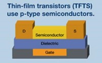
Scientists at Dongguk University have found a way to create printed p-channel thin-film transistors by using the abundantly available and environmentally friendly copper(I) iodide semiconductor at room temperature. Their energy-efficient and cost-effective fabrication method for these transistors may pave the way for developing low-cost and novel optoelectronic devices.
Transistors are the building blocks of most of the electronic devices we use every day, and research on fabricating new types of semiconducting materials for thin-film transistors (TFIs) has been ongoing for decades. Whenever new transistors or novel fabrication methods are discovered, many previously impossible applications become feasible, such as ultrahigh-definition transparent displays and flexible electronic devices. Nowadays, there is a huge demand for p-type transparent semiconductors (which are conductive due to the movement of charge carriers called “holes”) for making p-channel transistors, but when compared to the n-type counterparts, their use is limited by chemical instability and poor electric properties.
To overcome these limitations, a research team at Dongguk University led by Prof. Yong-Young Noh focused on developing a p-type transparent semiconductor for TFTs using a metal halide like copper(I) iodide (CuI), instead of metal oxide. “The naturally abundant and environment friendly constitutional elements of CuI make it more appropriate for large-scale printed transparent electronics. More importantly, CuI has a higher hole mobility than other p-type oxide-based semiconductors,” explains Prof. Noh.
However, CuI had been barely used as a semiconductor for TFTs because its hole concentration is so high that it results in uncontrollable conductivity (transistors are generally meant to be easily turned on and off at high speeds, that is, they are meant to be switchable from a conductive to a non-conductive state). Moreover, standard solution-based processing for making thin films generally requires a heat treatment called “annealing,” which is energy and time consuming.
The researchers found out that it is possible to reduce the conductivity of CuI-based thin films by making them even thinner and thus suitable for fabricating TFTs with the performance that is currently in demand for many applications. Additionally, these CuI thin films do not require annealing at all and can be processed at room temperature. This saves energy and makes them more cost-effective.
The team tested multiple processing conditions and fabricated various different TFTs to determine the origin of the enhanced device properties and to demonstrate the potential uses of CuI as a thin-film p-type semiconductor. “We believe that this work opens the floodgate for room-temperature, low-cost, printed transparent p-type transistors for diverse optoelectronic devices,” concludes Prof. Noh.
Share on:


Suggested Items
Designer’s Notebook: What Designers Need to Know About Manufacturing, Part 2
04/24/2024 | Vern Solberg -- Column: Designer's NotebookThe printed circuit board (PCB) is the primary base element for providing the interconnect platform for mounting and electrically joining electronic components. When assessing PCB design complexity, first consider the component area and board area ratio. If the surface area for the component interface is restricted, it may justify adopting multilayer or multilayer sequential buildup (SBU) PCB fabrication to enable a more efficient sub-surface circuit interconnect.
Insulectro’s 'Storekeepers' Extend Their Welcome to Technology Village at IPC APEX EXPO
04/03/2024 | InsulectroInsulectro, the largest distributor of materials for use in the manufacture of PCBs and printed electronics, welcomes attendees to its TECHNOLOGY VILLAGE during this year’s IPC APEX EXPO at the Anaheim Convention Center, April 9-11, 2024.
ENNOVI Introduces a New Flexible Circuit Production Process for Low Voltage Connectivity in EV Battery Cell Contacting Systems
04/03/2024 | PRNewswireENNOVI, a mobility electrification solutions partner, introduces a more advanced and sustainable way of producing flexible circuits for low voltage signals in electric vehicle (EV) battery cell contacting systems.
Heavy Copper PCBs: Bridging the Gap Between Design and Fabrication, Part 1
04/01/2024 | Yash Sutariya, Saturn Electronics ServicesThey call me Sparky. This is due to my talent for getting shocked by a variety of voltages and because I cannot seem to keep my hands out of power control cabinets. While I do not have the time to throw the knife switch to the off position, that doesn’t stop me from sticking screwdrivers into the fuse boxes. In all honesty, I’m lucky to be alive. Fortunately, I also have a talent for building high-voltage heavy copper circuit boards. Since this is where I spend most of my time, I can guide you through some potential design for manufacturability (DFM) hazards you may encounter with heavy copper design.
Trouble in Your Tank: Supporting IC Substrates and Advanced Packaging, Part 5
03/19/2024 | Michael Carano -- Column: Trouble in Your TankDirect metallization systems based on conductive graphite or carbon dispersion are quickly gaining acceptance worldwide. Indeed, the environmental and productivity gains one can achieve with these processes are outstanding. In today’s highly competitive and litigious environment, direct metallization reduces costs associated with compliance, waste treatment, and legal issues related to chemical exposure. What makes these processes leaders in the direct metallization space?