


 The Right Approach: I Hear the Train A Comin'
 It’s Only Common Sense: OCCAM—the Time Is Now
 Marcy's Musings: The Growing Industry
Controlling Charge Flow by Managing Electron Holes
February 7, 2019 | U.S. Department of Energy, Office of ScienceEstimated reading time: 2 minutes
Much remains to be learned about how charge moves along the molecules that make up the layers of materials in solar cells. These details have remained hidden because of the challenges of direct, real-time observation of motion of electrons and their holes at interfaces where two solar-cell materials meet.
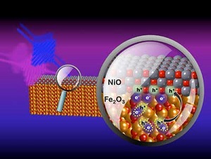
Image Caption: Researchers use extreme ultraviolet pulses (fuchsia line) to determine how visible light (blue line) causes interfacial hole (h+) transfer from iron oxide (Fe2O3) to nickel oxide (NiO), a hole collection layer commonly found in hybrid perovskite solar cells.
Using ultrafast extreme ultraviolet pulses, researchers watched as holes were injected across the interface materials found in hybrid perovskite solar cells. The bursts of extreme ultraviolet light were only femtoseconds in duration. The bursts allowed ultrafast, element-specific measurements.
The experiments revealed what states of the nickel atom are the primary hole-acceptors (Physical Chemistry Chemical Physics, "Identifying the acceptor state in NiO hole collection layers: Direct observation of exciton dissociation and interfacial hole transfer across a Fe2O3/NiO heterojunction").
Learning how charge moves in the material layers of solar cells could reveal missing design parameters. These parameters could let scientists control how charge moves inside solar panels or LEDs, including future designs based on novel materials.
Detailed knowledge of real-time motion of charge in solar-cell materials could help scientists and engineers design better solar cells. Here, scientists need to manage both electrons and the holes that are left behind. Specifically, they need a way to collect and move electron holes, the spots where electrons could be but aren’t.
But there’s a problem. The surface states of oxide materials that facilitate hole transfer are hard to study because it is difficult to probe directly between layers of materials, and the charge dynamics are extremely fast, making it difficult to follow them in real time.
Researchers devised a new way of examining charge transport within layered materials. Their new approach let them watch in real time how holes form and how the resulting electrons move, and they demonstrated the method by characterizing the interface formed with nickel oxide atop iron oxide.
The method employs extreme ultraviolet reflection–absorption spectroscopy using tiny bursts of extreme ultraviolet light only a few femtoseconds in duration. The short bursts allow real-time measurement of electron dynamics, and the burst energy allows element-specific measurements within layered materials.
They found that a transient nickel ion (Ni3+) forms after sunlight excites the underlying iron oxide layer. This tells the researchers how the holes in the nickel oxide work. In addition, the team’s work showed that holes are injected into the nickel oxide layer via a two-step process starting with a fast, field-driven exciton (electron-hole pair) dissociation in the iron layer.
With this research, scientists revealed the chemical nature of the hole acceptor state in nickel oxide. Also, they showed how exciton dissociation and interfacial hole transfer occur at the interface of nickel oxide and iron oxide, a model interface.
Share on:


Suggested Items
Real Time with... IPC APEX EXPO 2024: Sustainability in the Industry
04/26/2024 | Real Time with...IPC APEX EXPOGuest Editor Henry Crandall and Chris Nash of Indium Corporation discuss the company's 90th anniversary and its focus on sustainability. They focus on the benefits of sustainable materials, their compatibility, and value propositions. The conversation also highlights how Durafuse LT technology's role in reducing reflow temperatures is leading to significant cost and energy savings. Nash also touches on downstream sustainability efforts such as using recycled materials for packaging.
SMC Korea 2024 to Highlight Semiconductor Materials Trends and Innovations on Industry’s Path to $1 Trillion
04/24/2024 | SEMIWith Korea a major consumer of semiconductor materials and advanced materials a key driver of innovation on the industry’s path to $1 trillion, industry leaders and experts will gather at SMC (Strategic Materials Conference) Korea 2024 on May 29 at the Suwon Convention Center in Gyeonggi-do, South Korea to provide insights into the latest materials developments and trends. Registration is open.
Groundbreaking Ceremony Marks the Beginning of a New Era for Newccess Industrial; The Construction of the MINGXIN Building
04/12/2024 | Newccess IndustrialOn a clear and sunny day in March, the groundbreaking ceremony for the MINGXIN Building took place in Shenzhen, China. This moment marked the official commencement of construction for a project that will reshape the semiconductor materials industry.
The Need for a Holistic Global Sustainability Standard
04/10/2024 | Michael Ford, Aegis SoftwareNo one can deny that the resources of our fragile planet are finite. The environment seems like a third party, subject to constant degradation. We’re acutely aware of the effects of pollution on our climate, and despite our “throw-away” culture, recycling and recovery of materials has remained relatively expensive, even as we use more energy just to survive.
iNEMI Publishes Four Roadmap Topics
04/04/2024 | iNEMIThe International Electronics Manufacturing Initiative (iNEMI) announces the availability of the first roadmap topics in the new iNEMI Roadmap format. Printed circuit boards, sustainable electronics, smart manufacturing, and mmWave materials and test are now available online.