


 It’s Only Common Sense: OCCAM—the Time Is Now
 Marcy's Musings: The Growing Industry
 Dan’s Biz Bookshelf: Seeing the How
Using Artificial Intelligence to Engineer Materials’ Properties
February 12, 2019 | MITEstimated reading time: 6 minutes
Applying just a bit of strain to a piece of semiconductor or other crystalline material can deform the orderly arrangement of atoms in its structure enough to cause dramatic changes in its properties, such as the way it conducts electricity, transmits light, or conducts heat.
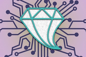
Image caption: Introducing a small amount of strain into crystalline materials, such as diamond or silicon, can produce significant changes in their properties, researchers have found. The mechanical strain is represented here as a deformation in the diamond's shape. Image: Chelsea Turner, MIT
Now, a team of researchers at MIT and in Russia and Singapore have found ways to use artificial intelligence to help predict and control these changes, potentially opening up new avenues of research on advanced materials for future high-tech devices.
The findings appear this week in the Proceedings of the National Academy of Sciences, in a paper authored by MIT professor of nuclear science and engineering and of materials science and engineering Ju Li, MIT Principal Research Scientist Ming Dao, and MIT graduate student Zhe Shi, with Evgeni Tsymbalov and Alexander Shapeev at the Skolkovo Institute of Science and Technology in Russia, and Subra Suresh, the Vannevar Bush Professor Emeritus and former dean of engineering at MIT and current president of Nanyang Technological University in Singapore.
Already, based on earlier work at MIT, some degree of elastic strain has been incorporated in some silicon processor chips. Even a 1% change in the structure can in some cases improve the speed of the device by 50%, by allowing electrons to move through the material faster.
Recent research by Suresh, Dao, and Yang Lu, a former MIT postdoc now at City University of Hong Kong, showed that even diamond, the strongest and hardest material found in nature, can be elastically stretched by as much as 9% without failure when it is in the form of nanometer-sized needles. Li and Yang similarly demonstrated that nanoscale wires of silicon can be stretched purely elastically by more than 15%. These discoveries have opened up new avenues to explore how devices can be fabricated with even more dramatic changes in the materials’ properties.
Strain Made to Order
Unlike other ways of changing a material’s properties, such as chemical doping, which produce a permanent, static change, strain engineering allows properties to be changed on the fly. “Strain is something you can turn on and off dynamically,” Li says.
But the potential of strain-engineered materials has been hampered by the daunting range of possibilities. Strain can be applied in any of six different ways (in three different dimensions, each one of which can produce strain in-and-out or sideways), and with nearly infinite gradations of degree, so the full range of possibilities is impractical to explore simply by trial and error. “It quickly grows to 100 million calculations if we want to map out the entire elastic strain space,” Li says.
Page 1 of 3
Share on:


Suggested Items
SMC Korea 2024 to Highlight Semiconductor Materials Trends and Innovations on Industry’s Path to $1 Trillion
04/24/2024 | SEMIWith Korea a major consumer of semiconductor materials and advanced materials a key driver of innovation on the industry’s path to $1 trillion, industry leaders and experts will gather at SMC (Strategic Materials Conference) Korea 2024 on May 29 at the Suwon Convention Center in Gyeonggi-do, South Korea to provide insights into the latest materials developments and trends. Registration is open.
Groundbreaking Ceremony Marks the Beginning of a New Era for Newccess Industrial; The Construction of the MINGXIN Building
04/12/2024 | Newccess IndustrialOn a clear and sunny day in March, the groundbreaking ceremony for the MINGXIN Building took place in Shenzhen, China. This moment marked the official commencement of construction for a project that will reshape the semiconductor materials industry.
The Need for a Holistic Global Sustainability Standard
04/10/2024 | Michael Ford, Aegis SoftwareNo one can deny that the resources of our fragile planet are finite. The environment seems like a third party, subject to constant degradation. We’re acutely aware of the effects of pollution on our climate, and despite our “throw-away” culture, recycling and recovery of materials has remained relatively expensive, even as we use more energy just to survive.
iNEMI Publishes Four Roadmap Topics
04/04/2024 | iNEMIThe International Electronics Manufacturing Initiative (iNEMI) announces the availability of the first roadmap topics in the new iNEMI Roadmap format. Printed circuit boards, sustainable electronics, smart manufacturing, and mmWave materials and test are now available online.
Insulectro’s 'Storekeepers' Extend Their Welcome to Technology Village at IPC APEX EXPO
04/03/2024 | InsulectroInsulectro, the largest distributor of materials for use in the manufacture of PCBs and printed electronics, welcomes attendees to its TECHNOLOGY VILLAGE during this year’s IPC APEX EXPO at the Anaheim Convention Center, April 9-11, 2024.