


 The Right Approach: I Hear the Train A Comin'
 It’s Only Common Sense: OCCAM—the Time Is Now
 Marcy's Musings: The Growing Industry
Collaboration Sparks Sustainable Electronics Manufacturing Breakthrough
February 14, 2019 | Simon Fraser UniversityEstimated reading time: 2 minutes
Simon Fraser University and Swiss researchers are developing an eco-friendly, 3D printable solution for producing wireless Internet-of-Things (IoT) sensors that can be used and disposed of without contaminating the environment.
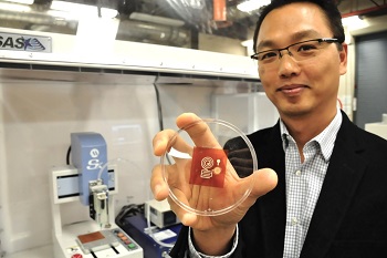
Image Caption: SFU Mechatronic Systems Engineering professor Woo Soo Kim is collaborating with Swiss researchers to develop an eco-friendly 3D printable solution for producing wireless Internet-of-Things sensors. The research team is using a wood-derived cellulose material to replace the plastics and polymeric materials currently used in electronics.
SFU professor Woo Soo Kim is leading the research team's discovery involving the use of a wood-derived cellulose material to replace the plastics and polymeric materials currently used in electronics.
Additionally, 3D printing can give flexibility to add or embed functions onto 3D shapes or textiles, creating greater functionality.
“Our eco-friendly 3D printed cellulose sensors can wirelessly transmit data during their life, and then can be disposed without concern of environmental contamination,” says Kim, a professor in the School of Mechatronic Systems Engineering. The SFU research is being carried out at PowerTech Labs in Surrey, which houses several state-of-the-art 3D printers used to advance the research.
“This development will help to advance green electronics. For example, the waste from printed circuit boards is a hazardous source of contamination to the environment. If we are able to change the plastics in PCB to cellulose composite materials, recycling of metal components on the board could be collected in a much easier way.”
Kim’s research program spans two international collaborative projects, including the latest focusing on the eco-friendly cellulose material-based chemical sensors with collaborators from the Swiss Federal Laboratories for Materials Science.
He is also collaborating with a team of South Korean researchers from the Daegu Gyeongbuk Institute of Science and Technology’s (DGIST)’s department of Robotics Engineering, and PROTEM Co Inc, a technology-based company, for the development of printable conductive ink materials.
In this second project, researchers have developed a new breakthrough in the embossing process technology, one that can freely imprint fine circuit patterns on flexible polymer substrate, a necessary component of electronic products.
Embossing technology is applied for the mass imprinting of precise patterns at a low unit cost. However, Kim says it can only imprint circuit patterns that are imprinted beforehand on the pattern stamp, and the entire, costly stamp must be changed to put in different patterns.
The team succeeded in developing a precise location control system that can imprint patterns directly resulting in a new process technology. The result will have widespread implications for use in semiconductor processes, wearable devices and the display industry.
Earlier this year Kim was selected as a Brain Pool Fellow by the National Research Foundation (NRF) of Korea.
An expert in 3D printed electronics who heads SFU’s Additive Manufacturing Laboratory, he spent six months collaborating with researchers at Seoul National University to advance fabrication of thin film transistors using 3D printing technology.
Share on:


Suggested Items
Warm Windows and Streamlined Skin Patches – IDTechEx Explores Flexible and Printed Electronics
04/26/2024 | IDTechExFlexible and printed electronics can be integrated into cars and homes to create modern aesthetics that are beneficial and easy to use. From luminous car controls to food labels that communicate the quality of food, the uses of this technology are endless and can upgrade many areas of everyday life.
iNEMI Packaging Tech Topic Series: Role of EDA in Advanced Semiconductor Packaging
04/26/2024 | iNEMIAdvanced semiconductor packaging with heterogenous integration has made on-package integration of multiple chips a crucial part of finding alternatives to transistor scaling. Historically, EDA tools for front-end and back-end design have evolved separately; however, design complexity and the increased number of die-to-die or die-to-substrate interconnections has led to the need for EDA tools that can support integration of overall design planning, implementation, and system analysis in a single cockpit.
Koh Young Showcases Award-winning Inspection Solutions at SMTconnect with SmartRep in Hall 4A.225
04/25/2024 | Koh Young TechnologyKoh Young Technology, the industry leader in True 3D measurement-based inspection solutions, will showcase an array of award-winning inspection and measurement solutions at SMTconnect alongside its sales partner, SmartRep, in booth 4A.225 at NürnbergMesse from June 11-13, 2023. The following offers a glimpse into what Koh Young will present at the tradeshow:
Real Time with… IPC APEX EXPO 2024: Plasmatreat: Innovative Surface Preparation Solutions
04/25/2024 | Real Time with...IPC APEX EXPOIn this interview, Editor Nolan Johnson speaks with Hardev Grewal, CEO and president of Plasmatreat, a developer of atmospheric plasma solutions. Plasmatreat uses clean compressed air and electricity to create plasma, offering environmentally friendly methods for surface preparation. Their technology measures plasma density for process optimization and can remove organic micro-contamination. Nolan and Hardev also discuss REDOX-Tool, a new technology for removing metal oxides.
Nanotechnology Market to Surpass $53.51 Billion by 2031
04/25/2024 | PRNewswireSkyQuest projects that the nanotechnology market will attain a value of USD 53.51 billion by 2031, with a CAGR of 36.4% over the forecast period (2024-2031).