


 It’s Only Common Sense: OCCAM—the Time Is Now
 Marcy's Musings: The Growing Industry
 Dan’s Biz Bookshelf: Seeing the How
Printed Radar Technology
February 27, 2019 | KITEstimated reading time: 4 minutes
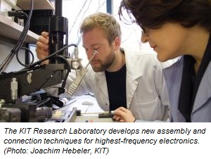
Parking a car with the help of radar sensors already is commonplace. Many other applications of radar technology are obvious, such as precise distance and environment sensors for robots and machines in the industrial automation sector or high-performance transmitters and receivers in telecommunications. Concrete application scenarios, however, are highly individual, the number of pieces is small, and manufacturing costs are very high. This is the point of departure of the new DiFeMiS Research Laboratory at Karlsruhe Institute of Technology (KIT). It is to develop print technologies for individual, small, and inexpensive high-frequency systems up to the terahertz range (THz). The Laboratory is funded by the Federal Ministry of Education and Research (BMBF) with about EUR 3.37 million.
When thinking of electronics, we mostly think of components on a green circuit board. But this carrier of electric components is suited for circuits working at frequencies far below 100 GHz only. At higher frequencies, boards are mainly produced by lithographic processes optimized for mass production. For medium batches of up to 10,000 products typically produced by small and medium-sized enterprises (SME), fabrication of an exposure mask for lithography is too expensive. Latest additive processes and precision printing technology might close this gap between individual and mass production.
“The core component of the planned Research Laboratory is a configurable, micrometer-precise printing platform for future highly flexible and inexpensive packaging,” says Professor Thomas Zwick, who heads KIT’s Institute of Radio Frequency Engineering and Electronics. Packaging or assembly and connection technology refers to all microchip-supporting components on a circuit board, from the conducting wire to the antenna. Packaging largely depends on the application, as far as the size and orientation of antennas are concerned, for instance. Hence, mass-produced off-the-shelf solutions are hardly suited. “At very high frequencies up to the terahertz range, radar technology is suited for many applications, as the high frequency enables increased measurement accuracy, higher data transmission rates, and further miniaturization.”
The Research Laboratory at KIT combines systems for additive and mask-less deposition and structuring methods in a flexible printing platform. Special measurement systems can be applied to determine the frequency behavior of components and systems at more than 500 GHz. To print electric circuits, several methods are available. Here, materials with various electric properties are applied as inks. These methods are two-dimensional, such ink-jet and aerosol-jet printing, or three-dimensional, such as laser lithography. For circuits above a frequency of 100 GHz, resolution has to be increased and complementary properties have to be combined. The big challenge lies in the exact positioning of components. For this purpose, printing processes are to be adjusted with micrometer precision, such that optimum collaboration of components from different printers is ensured and circuits are kept as small as possible.
SME might use digital manufacturing processes for inexpensive assembly and connection techniques at frequencies above 100 GHz in order to develop a large number of sensor applications for Industry 4.0 and robotics. Here, many measurement tasks have to be carried out, from simple distance measurements to complex imaging. Thanks to their good resolution, high accuracy, small size, and high robustness, high-frequency sensors are particularly suited for this purpose. Moreover, emitters and receivers based on high-frequency systems might be applied in telecommunications. Digital manufacturing might enable customized, integrated, and inexpensive production.
At KIT’s Research Laboratory, three research groups of Professors Thomas Zwick, Ulrich Lemmer, and Christian Koos from the Institute of Radio Frequency Engineering and Electronics, Light Technology Institute, and Institute of Photonics and Quantum Electronics are involved in DiFeMiS (German acronym of digital manufacture of THz microelectronics systems). The newly established chair of Ahmet Cagri Ulusoy at the Institute of Radio Frequency Engineering and Electronics is to join the project in the near future. The Laboratory will be funded by the Federal Ministry of Education and Research (BMBF) under the program “Microelectronics Research Laboratories in Germany” with EUR 3.37 million for a period of three years. Investments in most modern devices and facilities are to enable research on top international level. The twelve laboratories to be established under this program will open up new areas of research for future microelectronics and be used for training young scientists.
At today’s kick-off event, Thomas Rachel, Parliamentary State Secretary with the BMBF, underscored the importance of the research laboratories as an investment in the future. “We want to continue to live a self-determined life in a rapidly changing world. For this, Germany and Europe need to have a strong technological basis. The ‘Microelectronics Research Laboratories in Germany’ provide an essential contribution. At these laboratories, electronics for the next decades will be developed to maturity and new ideas and know-how will be transferred very quickly to everyday use.”
Being “The Research University in the Helmholtz Association“, KIT creates and imparts knowledge for the society and the environment. It is the objective to make significant contributions to the global challenges in the fields of energy, mobility and information. For this, about 9,300 employees cooperate in a broad range of disciplines in natural sciences, engineering sciences, economics, and the humanities and social sciences. KIT prepares its 25,100 students for responsible tasks in society, industry, and science by offering research-based study programs. Innovation efforts at KIT build a bridge between important scientific findings and their application for the benefit of society, economic prosperity, and the preservation of our natural basis of life.
Share on:


Suggested Items
Winner of The Science Show Rakett 69 Receives Incap Scholarship
04/24/2024 | IncapThe winner of the Rakett 69 science show, Andri Türkson, who stood out as an electronics enthusiast, received a scholarship from Incap Estonia, along with an internship opportunity in Saaremaa.
Alternative Manufacturing Inc. Awarded QML Requalification to IPC J-STD-001 and IPC-A-610
04/24/2024 | IPCIPC's Validation Services Program has awarded an IPC J-STD-001 and IPC-A-610 Qualified Manufacturers Listing (QML) requalification to Alternative Manufacturing Inc (AMI).
Boeing's Janene Stinson Earns IPC Excellence in Education Award at IPC APEX EXPO 2024
04/22/2024 | IPCThe IPC Excellence in Education award was presented to Janene Stinson, Boeing, at IPC APEX EXPO 2024 in Anaheim, California, in recognition of her significant contributions to workforce development and leadership.
Zentech’s Board of Directors Announces the Return of Matt Turpin as President and CEO
04/22/2024 | Zentech ManufacturingTurpin draws upon over 35 years of experience in the electronics industry and has an 18-year history with Zentech. He previously served as President and CEO from 2006 to 2019 after which time he has remained active in the EMS industry as an advisor to Zentech and other industry organizations.
IDTechEx Report Unveils 3D Electronics Status and Opportunities
04/22/2024 | PRNewswire3D electronics is an emerging manufacturing approach that enables electronics to be integrated within or onto the surface of objects. 3D electronic manufacturing techniques empower new features, including mass customizability, greater integration, and improved sustainability in the electronics industry.