


 The Right Approach: I Hear the Train A Comin'
 It’s Only Common Sense: OCCAM—the Time Is Now
 Marcy's Musings: The Growing Industry
Graphene Quantum Dots for Single Electron Transistors
March 7, 2019 | National Research University Higher School of EconomicsEstimated reading time: 1 minute
Scientists from the Higher School of Economics, Manchester University, the Ulsan National Institute of Science & Technology and the Korea Institute of Science and Technology have developed a novel technology, which combines the fabrication procedures of planar and vertical heterostructures in order to assemble graphene-based high-quality single-electron transistors. This technology could considerably expand the scope of research on two-dimensional materials by introducing a broader platform for the investigation of various devices and physical phenomena.
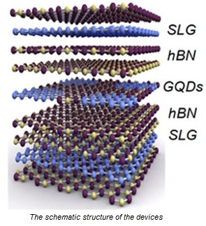
In the study, it was demonstrated that high-quality graphene quantum dots (GQDs), regardless of whether they were ordered or randomly distributed, could be successfully synthesised in a matrix of monolayer hexagonal boron nitride (hBN). Here, the growth of GQDs within the layer of hBN was shown to be catalytically supported by the platinum (Pt) nanoparticles distributed in-between the hBN and supporting oxidised silicon (SiO2) wafer, when the whole structure was treated by the heat in the methane gas (CH4). It was also shown, that due to the same lattice structure (hexagonal) and small lattice mismatch (~1.5%) of graphene and hBN, graphene islands grow in the hBN with passivated edge states, thereby giving rise to the formation of defectless quantum dots embedded in the hBN monolayer.
The Schematic Structure of the Devices
Such planar heterostructures incorporated by means of standard dry-transfer as mid-layers into the regular structure of vertical tunnelling transistors (Si/SiO2/hBN/Gr/hBN/GQDs/hBN/Gr/hBN; here Gr refers to monolayer graphene and GQDs refers to the layer of hBN with the embedded graphene quantum dots) were studied through tunnel spectroscopy at low temperatures (3He, 250mK). The study demonstrated where the manifestation of well-established phenomena of the Coulomb blockade for each graphene quantum dot as a separate single electron transmission channel occurs.
"Although the outstanding quality of our single electron transistors could be used for the development of future electronics," explains study co-author Davit Ghazaryan, associate professor at the HSE Faculty of Physics, and Research Fellow at the Institute of Solid State Physics (RAS). ‘This work is most valuable from a technological standpoint as it suggests a new platform for the investigation of physical properties of various materials through a combination of planar and van der Waals heterostructures.’
Share on:


Suggested Items
Koh Young Showcases Award-winning Inspection Solutions at SMTconnect with SmartRep in Hall 4A.225
04/25/2024 | Koh Young TechnologyKoh Young Technology, the industry leader in True 3D measurement-based inspection solutions, will showcase an array of award-winning inspection and measurement solutions at SMTconnect alongside its sales partner, SmartRep, in booth 4A.225 at NürnbergMesse from June 11-13, 2023. The following offers a glimpse into what Koh Young will present at the tradeshow:
Real Time with… IPC APEX EXPO 2024: Plasmatreat: Innovative Surface Preparation Solutions
04/25/2024 | Real Time with...IPC APEX EXPOIn this interview, Editor Nolan Johnson speaks with Hardev Grewal, CEO and president of Plasmatreat, a developer of atmospheric plasma solutions. Plasmatreat uses clean compressed air and electricity to create plasma, offering environmentally friendly methods for surface preparation. Their technology measures plasma density for process optimization and can remove organic micro-contamination. Nolan and Hardev also discuss REDOX-Tool, a new technology for removing metal oxides.
Nanotechnology Market to Surpass $53.51 Billion by 2031
04/25/2024 | PRNewswireSkyQuest projects that the nanotechnology market will attain a value of USD 53.51 billion by 2031, with a CAGR of 36.4% over the forecast period (2024-2031).
Cadence, TSMC Collaborate on Wide-Ranging Innovations to Transform System and Semiconductor Design
04/25/2024 | Cadence Design SystemsCadence Design Systems, Inc. and TSMC have extended their longstanding collaboration by announcing a broad range of innovative technology advancements to accelerate design, including developments ranging from 3D-IC and advanced process nodes to design IP and photonics.
SMC Korea 2024 to Highlight Semiconductor Materials Trends and Innovations on Industry’s Path to $1 Trillion
04/24/2024 | SEMIWith Korea a major consumer of semiconductor materials and advanced materials a key driver of innovation on the industry’s path to $1 trillion, industry leaders and experts will gather at SMC (Strategic Materials Conference) Korea 2024 on May 29 at the Suwon Convention Center in Gyeonggi-do, South Korea to provide insights into the latest materials developments and trends. Registration is open.