


 Marcy's Musings: The Growing Industry
 It’s Only Common Sense: Here’s What To Do After IPC APEX EXPO 2024
 Dan’s Biz Bookshelf: Seeing the How
Moiré Patterns of Three Layers Change the Electronic Properties of Graphene
March 11, 2019 | University of BaselEstimated reading time: 2 minutes
Combining an atomically thin graphene and a boron nitride layer at a slightly rotated angle changes their electrical properties. Physicists at the University of Basel have now shown for the first time the combination with a third layer can result in new material properties also in a three-layer sandwich of carbon and boron nitride. This significantly increases the number of potential synthetic materials, report the researchers in the scientific journal Nano Letters.
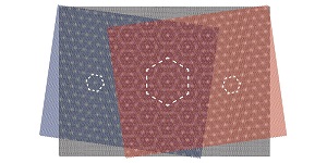
Image Caption: A graphene layer (black) of hexagonally arranged carbon atoms is placed between two layers of boron nitride atoms, which are also arranged hexagonally with a slightly different size. The overlap creates honeycomb patterns in various sizes. (Image: Swiss Nanoscience Institute, University of Basel).
Last year, researchers in the US caused a big stir when they showed that rotating two stacked graphene layers by a “magical” angle of 1.1 degrees turns graphene superconducting—a striking example of how the combination of atomically thin materials can produce completely new electrical properties.
Precision Alignment
Scientists from the Swiss Nanoscience Institute and the Department of Physics at the University of Basel have now taken this concept one step further. They placed a layer of graphene between two boron nitride layers, which is often serves to protect the sensitive carbon structure. Doing so, they aligned the layers very precisely with the crystal lattice of the graphene.
The effect observed by the physicists in Professor Christian Schönenberger’s team is commonly known as a moiré pattern: when two regular patterns are superimposed, a new pattern results with a larger periodic lattice.
New Three-Layer Superlattice
Lujun Wang, a member of the SNI PhD School and researcher in Schönenberger’s team, also observed effects of this kind of superlattice when he combined layers of boron nitride and graphene. The atoms are arranged hexagonally in all layers. If they are stacked on top of each other, larger regular patterns emerge, with a size depending on the angle between the layers.
It had already been shown that this works with a two-layer combination of graphene and boron nitride, but the effects due to a second boron nitride layer had not yet been found.
When the physicists from Basel experimented with three layers, two superlattices were formed between the graphene and the upper and the lower boron nitride layer, respectively. The superposition of all three layers created an even larger superstructure than possible with only one layer.
Scientists are very interested in these types of synthetic materials, since the different moiré patterns can be used to change or artificially produce new electronic material properties.
“To put it simply, the atomic patterns determine the behavior of electrons in a material, and we are combining different naturally occurring patterns to create new synthetic materials,” explains Dr. Andreas Baumgartner, who supervised the project. “Now we have discovered effects in these tailor-made electronic devices that are consistent with a three-layer superstructure,” he adds.
Share on:


Suggested Items
Groundbreaking Ceremony Marks the Beginning of a New Era for Newccess Industrial; The Construction of the MINGXIN Building
04/12/2024 | Newccess IndustrialOn a clear and sunny day in March, the groundbreaking ceremony for the MINGXIN Building took place in Shenzhen, China. This moment marked the official commencement of construction for a project that will reshape the semiconductor materials industry.
The Need for a Holistic Global Sustainability Standard
04/10/2024 | Michael Ford, Aegis SoftwareNo one can deny that the resources of our fragile planet are finite. The environment seems like a third party, subject to constant degradation. We’re acutely aware of the effects of pollution on our climate, and despite our “throw-away” culture, recycling and recovery of materials has remained relatively expensive, even as we use more energy just to survive.
iNEMI Publishes Four Roadmap Topics
04/04/2024 | iNEMIThe International Electronics Manufacturing Initiative (iNEMI) announces the availability of the first roadmap topics in the new iNEMI Roadmap format. Printed circuit boards, sustainable electronics, smart manufacturing, and mmWave materials and test are now available online.
Insulectro’s 'Storekeepers' Extend Their Welcome to Technology Village at IPC APEX EXPO
04/03/2024 | InsulectroInsulectro, the largest distributor of materials for use in the manufacture of PCBs and printed electronics, welcomes attendees to its TECHNOLOGY VILLAGE during this year’s IPC APEX EXPO at the Anaheim Convention Center, April 9-11, 2024.
Checking In With ICAPE Group
04/03/2024 | Nolan Johnson, I-Connect007ICAPE Group’s field application engineer Erik Pederson drills down on sustainability, supply chain resiliency, and what value engineering really looks like in this exclusive interview. Founded in 1999, European-based ICAPE Group provides 21 million printed circuit boards and over six million technical parts to manufacturers every month. With 30 PCB manufacturing partners globally and 50 partners providing a wide array of technical parts, ICAPE Group has operations in China, Taiwan, Thailand, South Korea, Vietnam, South Africa, Europe, Mexico, and the United States. The company also focuses on the value proposition for its customers.