


 Marcy's Musings: The Growing Industry
 It’s Only Common Sense: Here’s What To Do After IPC APEX EXPO 2024
 Dan’s Biz Bookshelf: Seeing the How
Tiny Optical Elements Could One Day Replace Traditional Refractive Lenses
March 29, 2019 | Northwestern UniversityEstimated reading time: 1 minute
A Northwestern University research team has developed tiny optical elements from metal nanoparticles and a polymer that one day could replace traditional refractive lenses to realize portable imaging systems and optoelectronic devices.
The flat and versatile lens, a type of metalens, has a thickness 100 times smaller than the width of a human hair.
“This miniaturization and integration with detectors offers promise for high-resolution imaging in devices from small wide-angle cameras to miniature endoscopes,” said Teri W. Odom, who led the research. She is the Charles E. and Emma H. Morrison Professor of Chemistry in the Weinberg College of Arts and Sciences and chair of the department of chemistry.
The properties of metalenses depend on the rationally designed arrangement of nanoscale units. Metalenses have emerged as an attractive option for flat lenses but are currently limited by their static, as-fabricated properties and their complex and expensive fabrication.
For imaging operations such as zooming and focusing, however, most metalenses cannot adjust their focal spots without physical motion. One major reason, Odom said, is that the building blocks of these lenses are made of hard materials that cannot change shape once fabricated. It is difficult in any materials systems to adjust nanoscale-sized features on demand to obtain tunable focusing in metalenses.
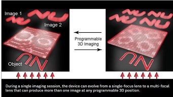
“In this study, we demonstrated a versatile imaging platform based on fully reconfigurable metalenses made from silver nanoparticles,” said Odom, a member of Northwestern’s International Institute for Nanotechnology. “During a single imaging session, our metalens device can evolve from a single-focus lens to a multi-focal lens that can form more than one image at any programmable 3D position.”
The paper, titled “Lattice-Resonance Metalenses for Fully Reconfigurable Imaging,” was published recently by the journal ACS Nano.
The Northwestern team built their lenses out of an array of cylindrical silver nanoparticles and a layer of polymer patterned into blocks on top of the metal array. By simply controlling the arrangement of the polymer patterns, the nanoparticle array could direct visible light to any targeted focal points without needing to change the nanoparticle structures.
This scalable method enables different lens structures to be made in one step of erasing and writing, with no noticeable degradation in nanoscale features after multiple erase-and-write cycles. The technique that can reshape any pre-formed polymer pattern into any desirable pattern using soft masks made from elastomers.
Share on:


Suggested Items
Inkjet Solder Mask ‘Has Arrived’
04/10/2024 | Pete Starkey, I-Connect007I was delighted to be invited to attend an interactive webinar entitled “Solder Mask Coating Made Easy with Additive Manufacturing,” hosted by SUSS MicroTec Netherlands in Eindhoven. The webinar was introduced and moderated by André Bodegom, managing director at Adeon Technologies, and the speakers were Mariana Van Dam, senior product manager PCB imaging solutions at AGFA in Belgium; Ashley Steers, sales manager at Electra Polymers in the UK; and Dr. Luca Gautero, product manager at SUSS MicroTec Netherlands.
NetVia Group Acquires Direct Imaging from Mivatek
04/09/2024 | Miva TechnologiesMiva Technologies is pleased to announce NetVia Group, Irving, TX has acquired a new Miva 2400NG Dual Tray Direct Imaging System with 30-micron capabilities for inner, outer and soldermask imaging.
Teledyne to Acquire Adimec
02/13/2024 | TeledyneTeledyne Technologies Incorporated announced that it has entered into an agreement to acquire Adimec Holding B.V. and its subsidiaries.
Real Time with... productronica 2023: MivaTek Global Advances Technology With High-res Imaging System
12/08/2023 | Real Time with...productronicaMivaTek's Brendan Hogan talks about how the company employs Digitally Adaptive Rasterization Technology (DART) in their high-res imaging equipment. He also shares how the blurred line between semiconductors and microelectronics is driving broader application of the imaging process.
Keysight Enables Validation of Arbe 4D Imaging Radar Chipset
11/30/2023 | Keysight Technologies, Inc.Keysight Technologies, Inc. announces that Arbe has selected the E8719A Radar Target Solution (RTS) to test the Arbe 4D imaging radar chipset for automotive applications.