


 Marcy's Musings: The Growing Industry
 It’s Only Common Sense: Here’s What To Do After IPC APEX EXPO 2024
 Dan’s Biz Bookshelf: Seeing the How
PV Nano Cell Shares Insights Following Best Ever Exhibition at LOPEC 2019
April 3, 2019 | Globe NewswireEstimated reading time: 2 minutes
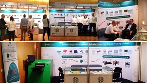
PV Nano Cell, Ltd. has announced its successful exhibition at LOPEC 2019, the leading event for Printed Electronics in Europe.
PV Nano Cell launched at the exhibition its complete solution offering for printed electronics, mass-production applications. The solution includes 3 critical components: inks, printers and printing process. The company's booth was visited by hundreds of prospects and significant leads were generated.
PV Nano Cell’s Chief of Business Development, Hanan Markovich, commented: “The exhibition was the best ever for us with an increase of 44% in total qualified registered leads compared to those registered last year. An Overwhelming 87% of the visitors to our booth work at industry-related companies whereas the rest work at research institutes and academia-related companies. More than a third of the visitors expressed high interest in mass-production applications. Furthermore, nearly half of all enquiries were made regarding a complete solution involving the ink, printer and printing process. This proves customers require a complete solution that addresses all aspects of conductive printing. Finally, the markets most discussed with us were: Automotive, PCB and Sensors. The interest in these markets demonstrates the promising, mass-production direction the industry is heading towards."
PV Nano Cell also presented its new and unique ink development for LIFT (Laser Induced Forward Transfer). The ink received significant attention from visitors and will be incorporated in the new catalog by Sigma-Aldrich. During the exhibition PV Nano Cell also demonstrated its integrated printer for design, prototyping and R&D – DemonJet.
As part of its solution strategy, the Company not only offers inks and printers but also develops the printing process for the customer. The printing process relates to the recipe, fine details and know-how of using the printer and ink to obtain the desired results for mass-production, 24/7 printing. Such know-how may include: ink properties' tweaking, printer parameters setup, printer modifications, tailored sintering instructions and more.
“This exhibition has boosted our potential customer base, especially for high volume ink consumption commercial applications and for our DemonJet™ printer. We hope the efforts we will invest in these leads in the coming months will be reflected as a rapid increase of our revenues, keeping the pace with last year’s growth,” commented Dr. Fernando de la Vega, PV Nano Cell CEO.
About PV Nano Cell, Ltd.
PV Nano Cell has developed innovative conductive inks for use in printed electronics (PE) and solar photovoltaics (PV) applications. PV Nano Cell's Sicrys™ ink family is a single-crystal, nano metric metal conductive ink delivering enhanced performance. Sicrys™ is available in silver and copper-based form, both compatible with many inkjet print heads and mass production enablers (high throughput printing, high quality and competitive pricing). Sicrys™ conductive inks are used all over the world in a range of inkjet printing applications, including photovoltaics, printed circuit boards, antennas, sensors, touchscreens and other applications.
Share on:


Suggested Items
Insulectro’s 'Storekeepers' Extend Their Welcome to Technology Village at IPC APEX EXPO
04/03/2024 | InsulectroInsulectro, the largest distributor of materials for use in the manufacture of PCBs and printed electronics, welcomes attendees to its TECHNOLOGY VILLAGE during this year’s IPC APEX EXPO at the Anaheim Convention Center, April 9-11, 2024.
ENNOVI Introduces a New Flexible Circuit Production Process for Low Voltage Connectivity in EV Battery Cell Contacting Systems
04/03/2024 | PRNewswireENNOVI, a mobility electrification solutions partner, introduces a more advanced and sustainable way of producing flexible circuits for low voltage signals in electric vehicle (EV) battery cell contacting systems.
Heavy Copper PCBs: Bridging the Gap Between Design and Fabrication, Part 1
04/01/2024 | Yash Sutariya, Saturn Electronics ServicesThey call me Sparky. This is due to my talent for getting shocked by a variety of voltages and because I cannot seem to keep my hands out of power control cabinets. While I do not have the time to throw the knife switch to the off position, that doesn’t stop me from sticking screwdrivers into the fuse boxes. In all honesty, I’m lucky to be alive. Fortunately, I also have a talent for building high-voltage heavy copper circuit boards. Since this is where I spend most of my time, I can guide you through some potential design for manufacturability (DFM) hazards you may encounter with heavy copper design.
Trouble in Your Tank: Supporting IC Substrates and Advanced Packaging, Part 5
03/19/2024 | Michael Carano -- Column: Trouble in Your TankDirect metallization systems based on conductive graphite or carbon dispersion are quickly gaining acceptance worldwide. Indeed, the environmental and productivity gains one can achieve with these processes are outstanding. In today’s highly competitive and litigious environment, direct metallization reduces costs associated with compliance, waste treatment, and legal issues related to chemical exposure. What makes these processes leaders in the direct metallization space?
AT&S Shines with Purest Copper on World Recycling Day
03/18/2024 | AT&SThe Styrian microelectronics specialist AT&S is taking World Recycling Day as an opportunity to review the progress that has been made in recent months at its sites around the world in terms of the efficient use of resources: