


 It’s Only Common Sense: OCCAM—the Time Is Now
 Marcy's Musings: The Growing Industry
 Dan’s Biz Bookshelf: Seeing the How
Squeezed Nanocrystals
April 8, 2019 | Ames LaboratoryEstimated reading time: 3 minutes
In a collaboration between the U.S. Department of Energy’s Ames Laboratory and Northeastern University, scientists have developed a model for predicting the shape of metal nanocrystals or “islands” sandwiched between or below two-dimensional (2D) materials such as graphene. The advance moves 2D quantum materials a step closer to applications in electronics.
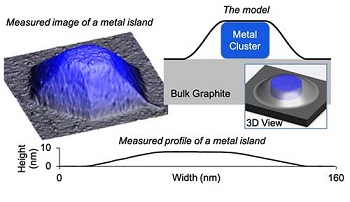
Image Caption: Ames Laboratory and Northeastern University developed and validated a model that predicts the shape of metal nanoparticles blanketed by 2D material. The top blanket of graphene resists deformation, "squeezing" downward on the metal nanoparticle and forcing it to be extremely low and wide.
Ames Laboratory scientist are experts in 2D materials, and recently discovered a first-of-its-kind copper and graphite combination, produced by depositing copper on ion-bombarded graphite at high temperature and in an ultra-high vacuum environment. This produced a distribution of copper islands, embedded under an ultra-thin “blanket” consisting of a few layers of graphene.
“Because these metal islands can potentially serve as electrical contacts or heat sinks in electronic applications, their shape and how they reach that shape are important pieces of information in controlling the design and synthesis of these materials,” said Pat Thiel, an Ames Laboratory scientist and Distinguished Professor of Chemistry and Materials Science and Engineering at Iowa State University.
Ames Laboratory and Northeastern University developed and validated a model that predicts the shape of metal nanoparticles blanketed by 2D material. The top blanket of graphene resists deformation, "squeezing" downward on the metal nanoparticle and forcing it to be extremely low and wide.
Ames Laboratory scientists used scanning tunneling microscopy to painstakingly measure the shapes of more than a hundred nanometer-scale copper islands. This provided the experimental basis for a theoretical model developed jointly by researchers at Northeastern University’s Department of Mechanical and Industrial Engineering and at Ames Laboratory. The model served to explain the data extremely well. The one exception, concerning copper islands less than 10 nm tall, will be the basis for further research.
“We love to see our physics applied, and this was a beautiful way to apply it,” said Scott E. Julien, Ph.D. candidate, at Northeastern. “We were able to model the elastic response of the graphene as it drapes over the copper islands, and use it to predict the shapes of the islands.”
The work showed that the top layer of graphene resists the upward pressure exerted by the growing metal island. In effect, the graphene layer squeezes downward and flattens the copper islands. Accounting for these effects as well as other key energetics leads to the unanticipated prediction of a universal, or size-independent, shape of the islands, at least for sufficiently-large islands of a given metal.
“This principle should work with other metals and other layered materials as well,” said Research Assistant, Ann Lii-Rosales. “Experimentally we want to see if we can use the same recipe to synthesize metals under other types of layered materials with predictable results.”
The research is further discussed in the paper, “Squeezed Nanocrystals: Equilibrium Configuration of Metal Clusters Embedded Beneath the Surface of a Layered Material,” authored by Scott E. Julien, Ann Lii-Rosales, Kai-Tak Wan, Yong Han, Michael C. Tringides, James W. Evans, and Patricia A. Thiel; and published in Nanoscale.
The research was a collaboration between Ames Laboratory and Northeastern University.
Work at Northeastern University was supported by the National Institute of Standards and Technology (NIST), a national facility operated under the U.S. Department of Commerce.
Work at Ames Laboratory was supported primarily by the U.S. Department of Energy Office of Science. This work was also supported in part by a grant of computer time at the National Energy Research Scientific Computing Centre (NERSC), a DOE Office of Science User Facility.
Ames Laboratory is a U.S. Department of Energy Office of Science national laboratory operated by Iowa State University. Ames Laboratory creates innovative materials, technologies and energy solutions. We use our expertise, unique capabilities and interdisciplinary collaborations to solve global problems.
DOE’s Office of Science is the single largest supporter of basic research in the physical sciences in the United States, and is working to address some of the most pressing challenges of our time.
Share on:


Suggested Items
Insulectro’s 'Storekeepers' Extend Their Welcome to Technology Village at IPC APEX EXPO
04/03/2024 | InsulectroInsulectro, the largest distributor of materials for use in the manufacture of PCBs and printed electronics, welcomes attendees to its TECHNOLOGY VILLAGE during this year’s IPC APEX EXPO at the Anaheim Convention Center, April 9-11, 2024.
ENNOVI Introduces a New Flexible Circuit Production Process for Low Voltage Connectivity in EV Battery Cell Contacting Systems
04/03/2024 | PRNewswireENNOVI, a mobility electrification solutions partner, introduces a more advanced and sustainable way of producing flexible circuits for low voltage signals in electric vehicle (EV) battery cell contacting systems.
Heavy Copper PCBs: Bridging the Gap Between Design and Fabrication, Part 1
04/01/2024 | Yash Sutariya, Saturn Electronics ServicesThey call me Sparky. This is due to my talent for getting shocked by a variety of voltages and because I cannot seem to keep my hands out of power control cabinets. While I do not have the time to throw the knife switch to the off position, that doesn’t stop me from sticking screwdrivers into the fuse boxes. In all honesty, I’m lucky to be alive. Fortunately, I also have a talent for building high-voltage heavy copper circuit boards. Since this is where I spend most of my time, I can guide you through some potential design for manufacturability (DFM) hazards you may encounter with heavy copper design.
Trouble in Your Tank: Supporting IC Substrates and Advanced Packaging, Part 5
03/19/2024 | Michael Carano -- Column: Trouble in Your TankDirect metallization systems based on conductive graphite or carbon dispersion are quickly gaining acceptance worldwide. Indeed, the environmental and productivity gains one can achieve with these processes are outstanding. In today’s highly competitive and litigious environment, direct metallization reduces costs associated with compliance, waste treatment, and legal issues related to chemical exposure. What makes these processes leaders in the direct metallization space?
AT&S Shines with Purest Copper on World Recycling Day
03/18/2024 | AT&SThe Styrian microelectronics specialist AT&S is taking World Recycling Day as an opportunity to review the progress that has been made in recent months at its sites around the world in terms of the efficient use of resources: