


 The Right Approach: I Hear the Train A Comin'
 It’s Only Common Sense: OCCAM—the Time Is Now
 Marcy's Musings: The Growing Industry
Measurement of Semiconductor Material Quality is Now 100,000 Times More Sensitive
April 10, 2019 | University of Texas at AustinEstimated reading time: 3 minutes
The enhanced power of the new measuring technique to characterize materials at scales much smaller than any current technologies will accelerate the discovery and investigation of 2D, micro- and nanoscale materials.
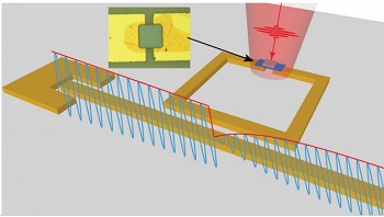
Image Caption: Rendering of microwave resonator showing the (blue) microwave signal’s size change resulting from a light pulse (red) once the pulse hits the infrared pixel (micrograph image of pixel is shown in the inset).
Being able to accurately measure semiconductor properties of materials in small volumes helps engineers determine the range of applications for which these materials may be suitable in the future, particularly as the size of electronic and optical devices continues to shrink.
Daniel Wasserman, an associate professor in the Department of Electrical and Computer Engineering in the Cockrell School of Engineering, led the team that built the physical system, developed the measurement technique capable of achieving this level of sensitivity and successfully demonstrated its improved performance. Their work was reported today in Nature Communications.
The team’s design approach was focused on developing the capability to provide quantitative feedback on material quality, with particular applications for the development and manufacturing of optoelectronic devices. The method demonstrated is capable of measuring many of the materials that engineers believe will one day be ubiquitous to next-generation optoelectronic devices.
Optoelectronics is the study and application of electronic devices that can source, detect and control light. Optoelectronic devices that detect light, known as photodetectors, use materials that generate electrical signals from light. Photodetectors are found in smartphone cameras, solar cells and in the fiber optic communication systems that make up our broadband networks. In an optoelectronic material, the amount of time that the electrons remain “photoexcited,” or capable of producing an electrical signal, is a reliable indicator of the potential quality of that material for photodetection applications.
The current method used for measuring the carrier dynamics, or lifetimes, of photoexcited electrons is costly and complex and only measures large-scale material samples with limited accuracy. The UT team decided to try using a different method for quantifying these lifetimes by placing small volumes of the materials in specially designed microwave resonator circuits. Samples are exposed to concentrated microwave fields while inside the resonator. When the sample is hit with light, the microwave circuit signal changes, and the change in the circuit can be read out on a standard oscilloscope. The decay of the microwave signal indicates the lifetimes of photoexcited charge carriers in small volumes of the material placed in the circuit.
“Measuring the decay of the electrical (microwave) signal allows us to measure the materials’ carrier lifetime with far greater accuracy,” Wasserman said. “We have discovered it to be a simpler, cheaper and more effective method than current approaches.”
Carrier lifetime is a critical material parameter that provides insight into the overall optical quality of a material while also determining the range of applications for which a material could be used when it's integrated into a photodetector device structure. For example, materials that have a very long carrier lifetime may be of high optical quality and therefore very sensitive, but may not be useful for applications that require high-speed.
“Despite the importance of carrier lifetime, there are not many, if any, contact-free options for characterizing small-area materials such as infrared pixels or 2D materials, which have gained popularity and technological importance in recent years,” Wasserman said.
One area certain to benefit from the real-world applications of this technology is infrared detection, a vital component in molecular sensing, thermal imaging and certain defense and security systems.
“A better understanding of infrared materials could lead to innovations in night-vision goggles or infrared spectroscopy and sensing systems,” Wasserman said.
High-speed detectors operating at these frequencies could even enable the development of free-space communication in the long wavelength infrared – a technology allowing for wireless communication in difficult conditions, in space or between buildings in urban environments.
The research was funded by Air Force Research Laboratories and is part of an ongoing collaboration between Wasserman and his Mid-IR Photonics Group at UT, close collaborators at Eglin Air Force Base and researchers from The Ohio State University, University of Wisconsin and Sandia National Laboratories.
Share on:


Suggested Items
SMC Korea 2024 to Highlight Semiconductor Materials Trends and Innovations on Industry’s Path to $1 Trillion
04/24/2024 | SEMIWith Korea a major consumer of semiconductor materials and advanced materials a key driver of innovation on the industry’s path to $1 trillion, industry leaders and experts will gather at SMC (Strategic Materials Conference) Korea 2024 on May 29 at the Suwon Convention Center in Gyeonggi-do, South Korea to provide insights into the latest materials developments and trends. Registration is open.
Groundbreaking Ceremony Marks the Beginning of a New Era for Newccess Industrial; The Construction of the MINGXIN Building
04/12/2024 | Newccess IndustrialOn a clear and sunny day in March, the groundbreaking ceremony for the MINGXIN Building took place in Shenzhen, China. This moment marked the official commencement of construction for a project that will reshape the semiconductor materials industry.
The Need for a Holistic Global Sustainability Standard
04/10/2024 | Michael Ford, Aegis SoftwareNo one can deny that the resources of our fragile planet are finite. The environment seems like a third party, subject to constant degradation. We’re acutely aware of the effects of pollution on our climate, and despite our “throw-away” culture, recycling and recovery of materials has remained relatively expensive, even as we use more energy just to survive.
iNEMI Publishes Four Roadmap Topics
04/04/2024 | iNEMIThe International Electronics Manufacturing Initiative (iNEMI) announces the availability of the first roadmap topics in the new iNEMI Roadmap format. Printed circuit boards, sustainable electronics, smart manufacturing, and mmWave materials and test are now available online.
Insulectro’s 'Storekeepers' Extend Their Welcome to Technology Village at IPC APEX EXPO
04/03/2024 | InsulectroInsulectro, the largest distributor of materials for use in the manufacture of PCBs and printed electronics, welcomes attendees to its TECHNOLOGY VILLAGE during this year’s IPC APEX EXPO at the Anaheim Convention Center, April 9-11, 2024.